PCIe Compliance Testing Reference
PRELIMINARY INFORMATION
Jetson AGX Orin Series Tuning and Compliance Guide DA-11040-001_v0.7 | 22
Tx Test
For the Tx test, the PCIe specification describes a mechanism for testing the electrical
characteristics, which relies on a 50 Ω termination on the transmit lane to be tested.
Therefore, when the transmit lanes of the device are terminated with a 50 Ω termination, the
transmit lanes will automatically be forced into compliance mode. In this setup, the 50 Ω probe
termination on Tx lane-n under test will force compliance mode.
Make sure to apply PCIe controller always-on patch (PATCH-A) and apply REFCLK SSC disable
patch (PATCH-B) when needed. The patched OS must be flashed before test and then system
must boot from flash.
Steps for Gen1 to Gen3 Tx compliance testing are as follows:
1. Make sure wiring as per” Tx Test Setup” is complete.
2. Turn on the power supply powering CBB or turn on pulse generator.
3. Power on DUT, and boot into (patched) OS.
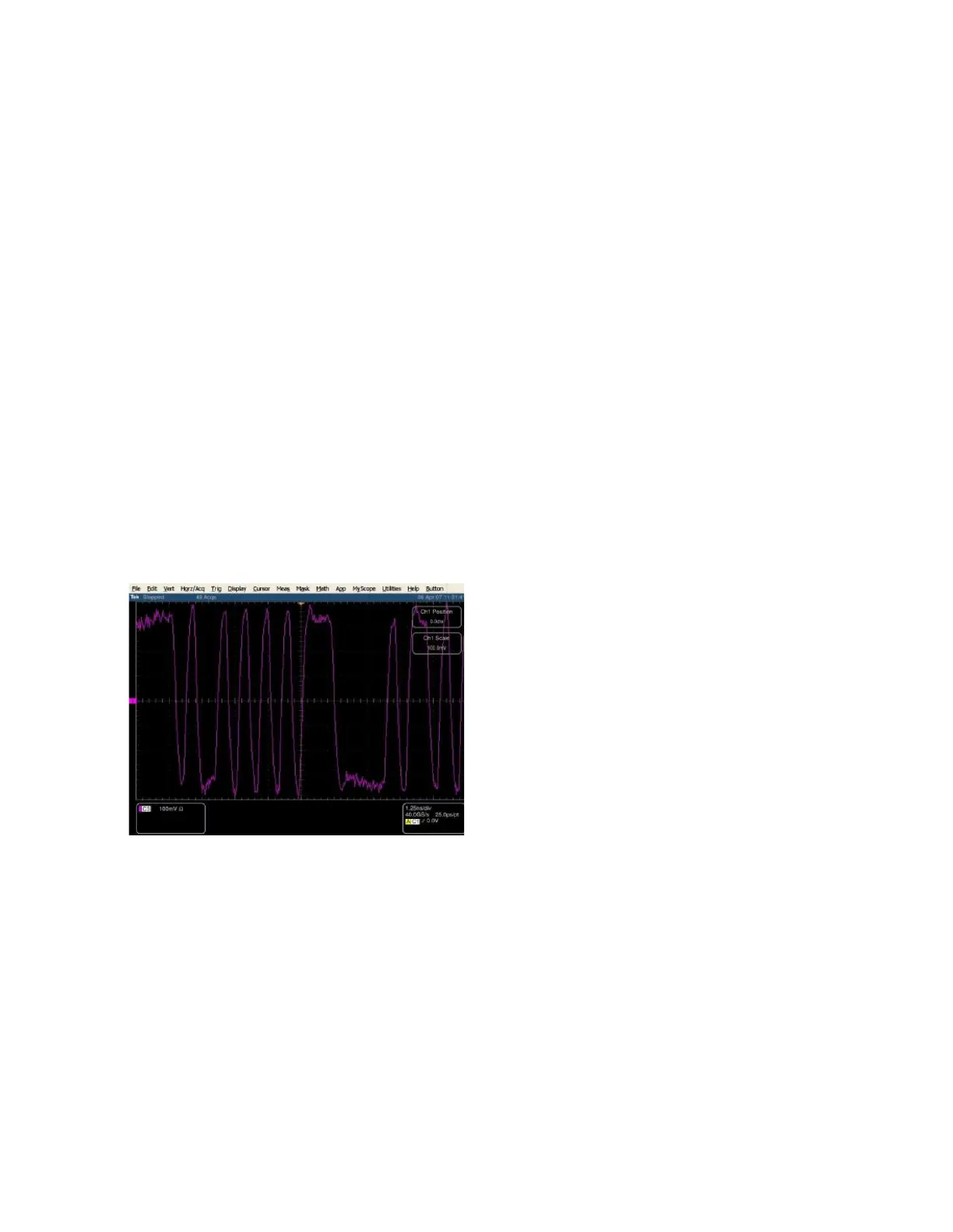
4. Use differential mode on scope, data CH1-CH3 and CLOCK CH2-CH4.
5. Adjust the horizontal scale on the scope, so that the data signal differential waveform is
clearly visible as shown in Figure 7.
Figure 7. Differential Data Signal Waveform
6. Set scope scale (20 us)/Bandwidth (13 G at least)/memory depth (10 M)/Sample rate (40 G).
7. Device with lane-n under test shall come up in Gen1 preset. Check scope REFCLK and
data lanes to make sure that Gen1 preset is achieved. After each new preset, check scope
REFCLK and data lanes to make sure that proper presets are achieved.
8. Capture the waveform corresponding to PCIe Gen1, Gen2, and Gen3 for all presets (Gen1-
1, Gen2-2, and Gen3-10 presets), move to different PCIe preset by inserting trigger pulse
on Rx line. For example, by pressing the CBB toggle button. (first toggle will move from
Gen1 to Gen 2-1). Make sure that the user interface numbers meet the following
requirements:
a). Gen1, 10E6 × 400.0 ps = 400.0 μs
b). Gen2, 10E6 × 200.0 ps = 200.0 μs

 Loading...