PCIe Compliance Testing Reference
PRELIMINARY INFORMATION
Jetson AGX Orin Series Tuning and Compliance Guide DA-11040-001_v0.7 | 23
c). Gen3, 10E6 × 200.0 ps = 200.0 μs
d). Check that the pattern on the scope is intended compliance pattern as specified by the
PCIe Base Specification
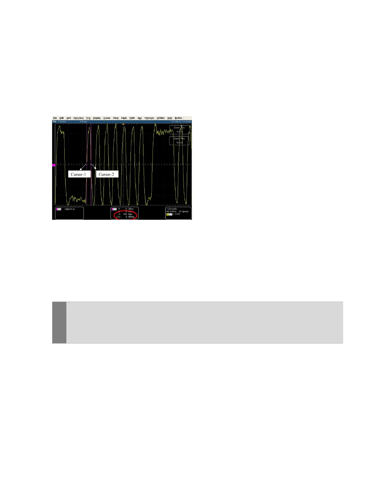
. The default the compliance pattern is sent at 2.5 GT/s (initial
state with no prior mode change). Use cursors shown in Figure 8 on a pair of adjacent
crossover locations to make sure that the user interface reflects the expected preset.
Figure 8. Gen1 Data Signal at 2.5 GT/s Showing user interface = 400 ps
9. Capture 100 M REFCLK waveform file and store it for post processing. In case spread
Spectrum is enabled on REFCLK, then REFCLK shall be captured simultaneously along
with data lane on a different channel.
10. Run post processing (for example, by Sigtest) by loading the Tx waveform file and clock
file. Once post processing (for example, SIGETST) proves result then a report must be
generated. When using Sigtest, it will generate reports by a script.
11. Toggle the button and change compliance pattern sequence and start the capture process
again.
!
CAUTION: Compliance testing and characterization as described in this application note apply to
PCIe Gen1 to Gen3 only. Applying this method to Gen4 may introduce additional noise due to
wiring of the breakout boards and running at Gen4 frequencies.
The following steps for Gen 4 Tx compliance testing are for reference only.
Steps for Gen4 Tx compliance testing are as follows and for reference only:
For PCIe Gen4, customers may repeat the steps described Gen1 to Gen3 with the following
modifications and additions:
Note that the sequence of modified and additional steps are to fit in with the steps for Gen1 to
Gen3.
1. Set scale (12.5 us), bandwidth (25 G at least), memory depth (10 M), and sample rate (80 G).
2. Capture the waveform corresponding to PCIe Gen4. For all Gen4 presets move to different
PCIe preset by inserting trigger pulse on Rx line by pressing the CBB toggle button. From

 Loading...