3 I/O Specifications and Wiring for Pulse I/O Modules
3-4
CJ2M CPU Unit Pulse I/O Module User’s Manual
z Normal Outputs (OUT00 to OUT05 and OUT10 to OUT15)
*Refer to 4-3-2 Wiring Examples for details on suppressing the load's inrush current and modify the circuit if nec-
essary.
z Pulse Outputs (OUT00 to OUT03 and OUT10 to OUT13)
Note The ON/OFF status given above is for the output element.
Additional Information
• The load for the above values is assumed to be the resistance load, and does not take into
account the impedance for the connecting cable to the load.
• Due to distortions in pulse waveforms resulting from connecting cable impedance, the pulse
widths in actual operation may be smaller than the values shown above.
3-1-2 Output Specifications for Sinking Transistor Outputs
Output Specifications
Rated voltage 5 to 24 VDC
Allowable voltage range 4.75 to 26.4 VDC
Maximum switching current 0.3 A/output; 1.8 A/Unit
Number of circuits 6 outputs (6 outputs/common)
Maximum inrush current 3.0 A/output, 10 ms max.*
Leakage current 0.1 mA max.
Residual voltage 0.6 V max.
ON response time 0.1 ms max.
OFF response time 0.1 ms max.
Fuse None
External power supply (power
supply input +V for outputs)
10.2 to 26.4 VDC 20 mA min.
Item Specifications
Rated voltage 5 to 24 VDC
Allowable voltage range 4.75 to 26.4 VDC
Maximum switching capacity 30 mA
Minimum switching capacity 7 mA
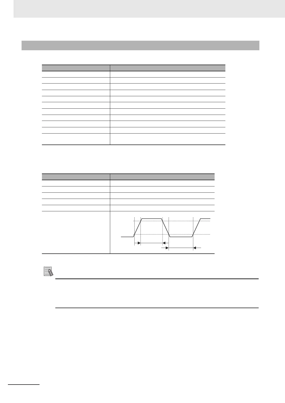
Maximum output frequency 100 kHz
Output waveform
90%
10%
OFF
ON
2 µs min.
4 µs min.
 Loading...