3-5
3 I/O Specifications and Wiring for Pulse I/O Modules
CJ2M CPU Unit Pulse I/O Module User’s Manual
3-1 I/O Specifications
3
3-1-3 Output Specifications for Sourcing Transistor Outputs
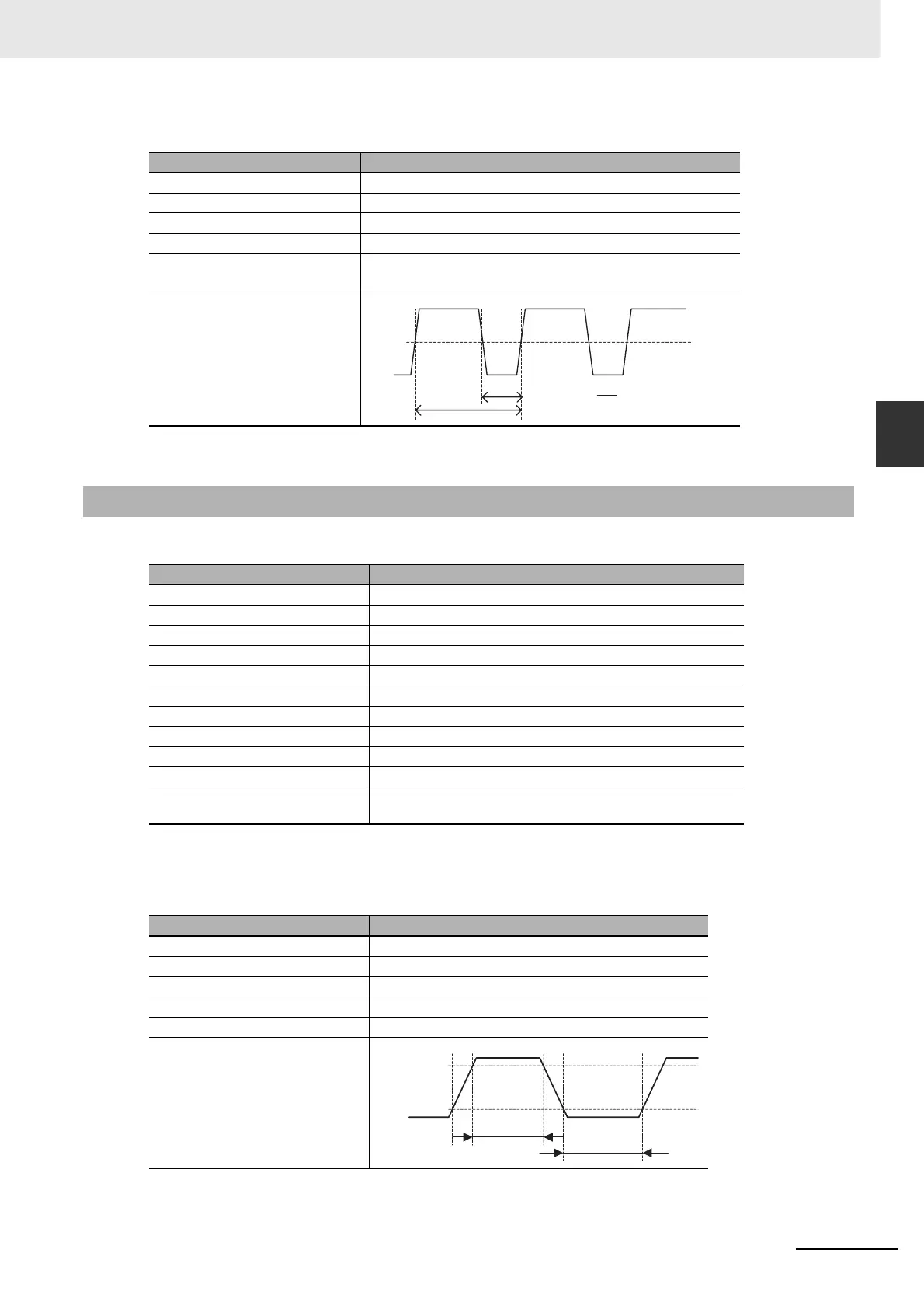
z PWM Outputs (OUT04, OUT05, OUT14, and OUT15)
Note The ON/OFF status given above is for the output element.
z Normal Outputs (OUT00 to OUT05 and OUT10 to OUT15)
*Refer to 4-3-2 Wiring Examples for details on suppressing the load's inrush current and modify the circuit if nec-
essary.
z Pulse Outputs (OUT00 to OUT03 and OUT10 to OUT13)
Note The ON/OFF status given above is for the output element.
Item Specifications
Rated voltage 5 to 24 VDC
Allowable voltage range 4.75 to 26.4 VDC
Maximum switching capacity 6.5535 kHz or less: 300 mA, 6.5535 to 32.8 kHz: 100 mA
Maximum output frequency 32,800 Hz
PWM output accuracy (for ON
pulse width of 2 µs or longer)
ON duty at 6.5535 kHz or less: −0.2% to +1%, ON duty at
32.8 kHz: −1% to +5% (at switching current of 30 mA)
Output waveform
3-1-3 Output Specifications for Sourcing Transistor Outputs
Output OUT0 to OUT5
Rated voltage 5 to 24 VDC
Operating load voltage range 4.75 to 26.4 VDC
Maximum switching current 0.3 A/output, 1.8 A/Unit
Number of circuits 6 outputs (6 outputs/common)
Maximum inrush current 2.0 A/output, 10 ms max.*
Leakage current 0.1 mA max.
Residual voltage 0.6 V max.
ON response time 0.1 ms max.
OFF response time 0.1 ms max.
Fuse None
External supply power (power
supply input −V for outputs)
10.2 to 26.4 VDC, 20 mA min.
Item Specifications
Rated voltage 5 to 24 VDC
Allowable voltage range 4.75 to 26.4 VDC
Maximum switching capacity 30 mA
Minimum switching capacity 7 mA
Maximum output frequency 100 kHz
Output waveform
ON
OFF
T
t
ON
50%
ON duty =
t
ON
T
X 100%
90%
10%
OFF
ON
4 µs min.
2 µs min.
 Loading...