LTE Standard Module Series
EC21_Series_Hardware_Design
26
/ 118
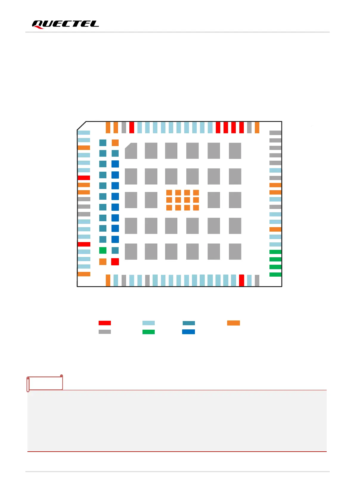
3.2. Pin Assignment
The following figure shows the pin assignment of EC21 series module.
34
3
35
36
20
21
22
23
24
25
26
27
28
29
30
31
32
33
1
4
5
6
7
2
WAKEUP_IN
AP_READY
RESERVED
W_DISABLE#
NET_MODE
NET_STATUS
VDD_EXT
GND
GND
DBG_RXD
DBG_TXD
USIM_PRESENCE
USIM_VDD
USIM_DATA
USIM_CLK
USIM_RST
RESERVED
8
9
10
11
12
13
14
15
16
17
18
19
54
53
52
51
50
49
48
47
46
45
44
43
42
41
40
39
38
37
72
71
70
69
68
67
66
65
64
63
62
61
60
59
58
57
56
55
USIM_GND
GND
RESET_N
PWRKEY
GND
SD_INS_DET
SDC2_DATA3
SDC2_DATA2
SDC2_DATA1
SDC2_DATA0
SDC2_CLK
SDC2_CMD
ANT_DIV
GND
GND
USB_VBUS
USB_DM
USB_DP
RXD
TXD
DTR
RTS
CTS
DCD
RI
STATUS
VBAT_BB
VBAT_BB
VBAT_RF
VBAT_RF
GND
RESERVED
GND
GND
ANT_MAIN
GND
ANT_GNSS
GND
ADC1
RESERVED
I2C_SDA
I2C_SCL
ADC0
GND
GND
GND
73
74
75
76
77
78
79
80
81
82
83
84
100
101
102
106
107
111
112
103
104
109
105
110
89
94
98
88
93
97
86
91
96
85
909599
8792
108
113
RESERVED
RESERVED
117
126
125
124
123
122
121
118
127
128
115
USB_BOOT
RESERVED
116
140
137
136
135
134
133
132
131
130
129
114
VDD_SDIO
Power Pins Signal Pins
GND Pins
RESERVED
RESERVED
141
142
RESERVED
RESERVED
143
144
119
120
WLAN Pins RESERVED Pins
Bluetooth Pins
PCM_IN
PCM_OUT
PCM_SYNC
PCM_CLK
BT_CTS
BT_RXD
BT_TXD
BT_RTS
139
138
SGMII Pins
Figure 2: Pin Assignment (Top View)
1. WAKEUP_IN, NET_MODE, WLAN_EN, COEX_UART_RX, COEX_UART_TX, USB_BOOT and
BT_CTS cannot be pulled up before startup.
2. PWRKEY output voltage is 0.8 V because of the diode drop in the baseband chipset.
3. Digital audio (PCM) is only supported on Data + Voice version.
4. Pins 37–40, 118, 127 and 129–139 are used for WLAN & Bluetooth application interfaces, among
which pins 118, 127 and 129–138 are WLAN function pins, and the rest of pins are Bluetooth
NOTE
 Loading...