LTE Standard Module Series
EC21_Series_Hardware_Design
80
/ 118
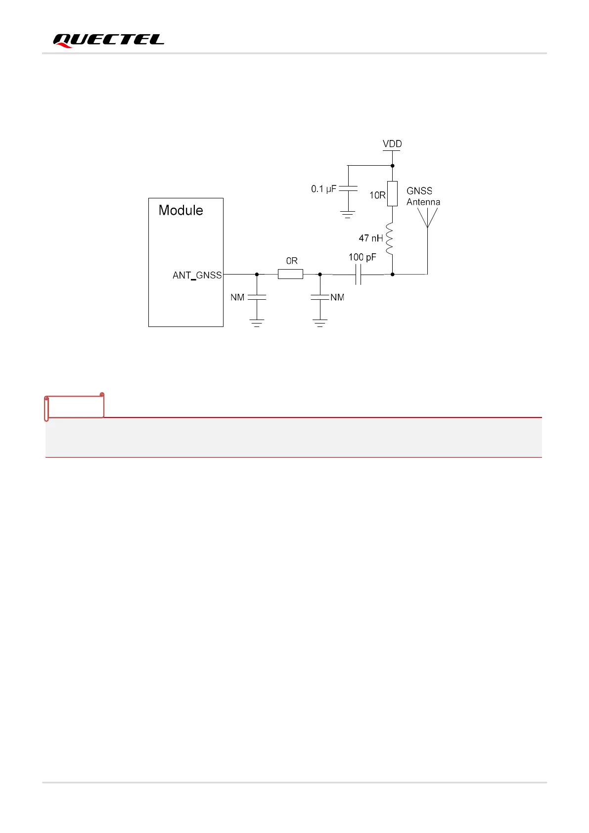
4.2.3. Reference Design
A reference design of GNSS antenna is shown as below.
Figure 34: Reference Circuit of GNSS Antenna
1. An external LDO can be selected to supply power according to the active antenna requirement.
2. If the module is designed with a passive antenna, then the VDD circuit is not needed.
4.2.4. Layout Guidelines
The following layout guidelines should be taken into account in customers’ designs.
Maximize the distance among GNSS antenna, main antenna and Rx-diversity antenna.
Digital circuits such as (U)SIM card, USB interface, camera module and display connector should be
kept away from the antennas.
Use ground vias around the GNSS trace and sensitive analog signal traces to provide coplanar
isolation and protection.
Keep 50 Ω characteristic impedance for the ANT_GNSS trace.
4.3. RF Routing Guidelines
For user’s PCB, the characteristic impedance of all RF traces should be controlled to 50 Ω. The
impedance of the RF traces is usually determined by the trace width (W), the materials’ dielectric
constant, the height from the reference ground to the signal layer (H), and the spacing between RF
NOTE
 Loading...