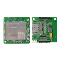
LTE Standard Module Series
EM05-G Hardware Design
EM05-G_Hardware_Design 26 / 69
For details of related AT commands, see document [3].
1. The W_DISABLE1# control function is disabled in firmware by default. It can be enabled by
AT+QCFG="airplanecontrol",1.
2. Execution of AT+CFUN will not affect GNSS function.
3.3. Power Supply
The following table shows pin definition of VCC and GND pins.
Table 7: Definition of VCC and GND Pins
3.3.1. Decrease Voltage Drop
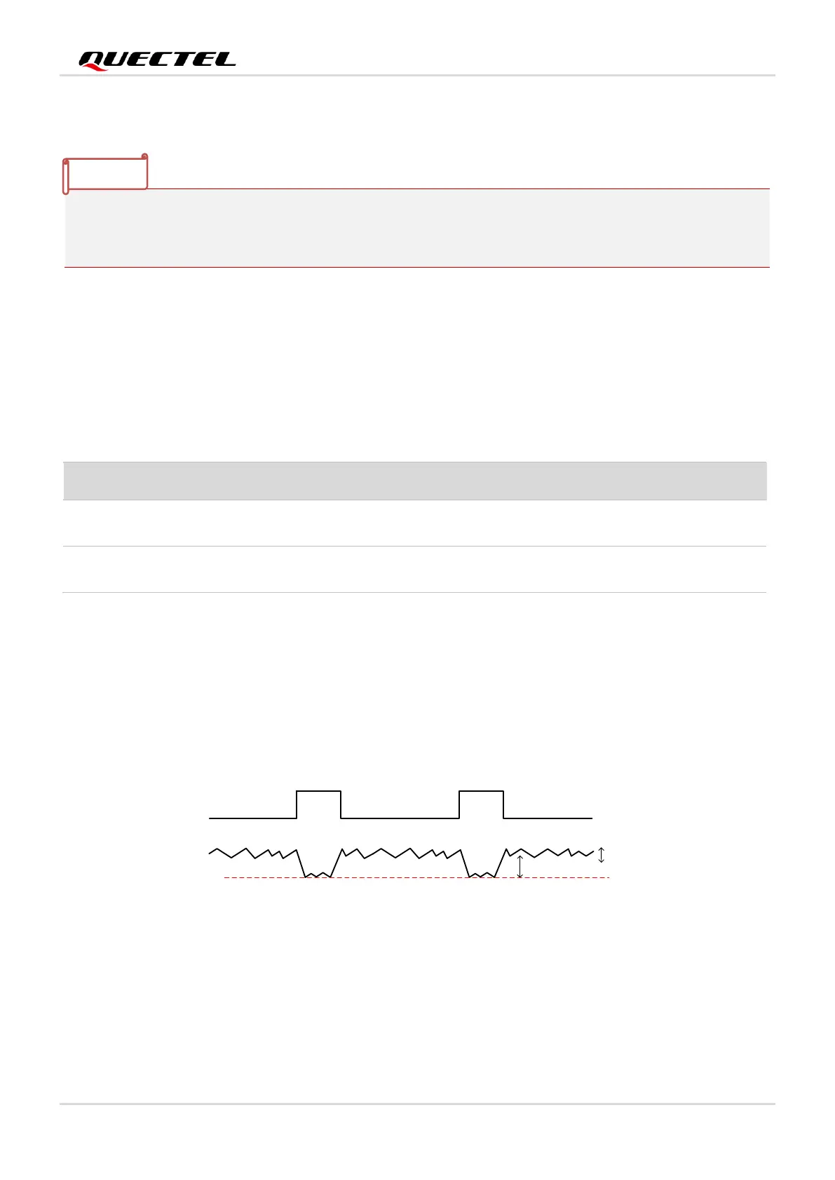
The power supply range of the module is from 3.135 V to 4.4 V. Please ensure that the input voltage will
never drop below 3.135 V, otherwise the module will be powered off automatically. The following figure
shows the maximum voltage drop during radio transmission in 3G/4G networks.
Power Supply
Burst Transmission
Ripple
Burst Transmission
Drop
Figure 6: Power Supply Limits during Radio Transmission
Ensure the continuous current capability of the power supply is 2.0 A. To decrease the voltage drop, two
bypass capacitor of about 220 µF with low ESR (ESR = 0.7 Ω) should be used. To decrease the power
supply is disturbed, a multi-layer ceramic chip capacitor (MLCC) array also should be used due to its
ultra-low ESR. It is recommended to use four ceramic capacitors (1 µF, 100 nF, 33 pF, 10 pF) for
3.135–4.4 V
3.3 V typical DC supply
3, 5, 11, 27, 33, 39, 45,
51, 57, 71, 73
 Loading...