UM2448 Rev 6 37/49
UM2448 B-STLINK-VOLT board extension description
48
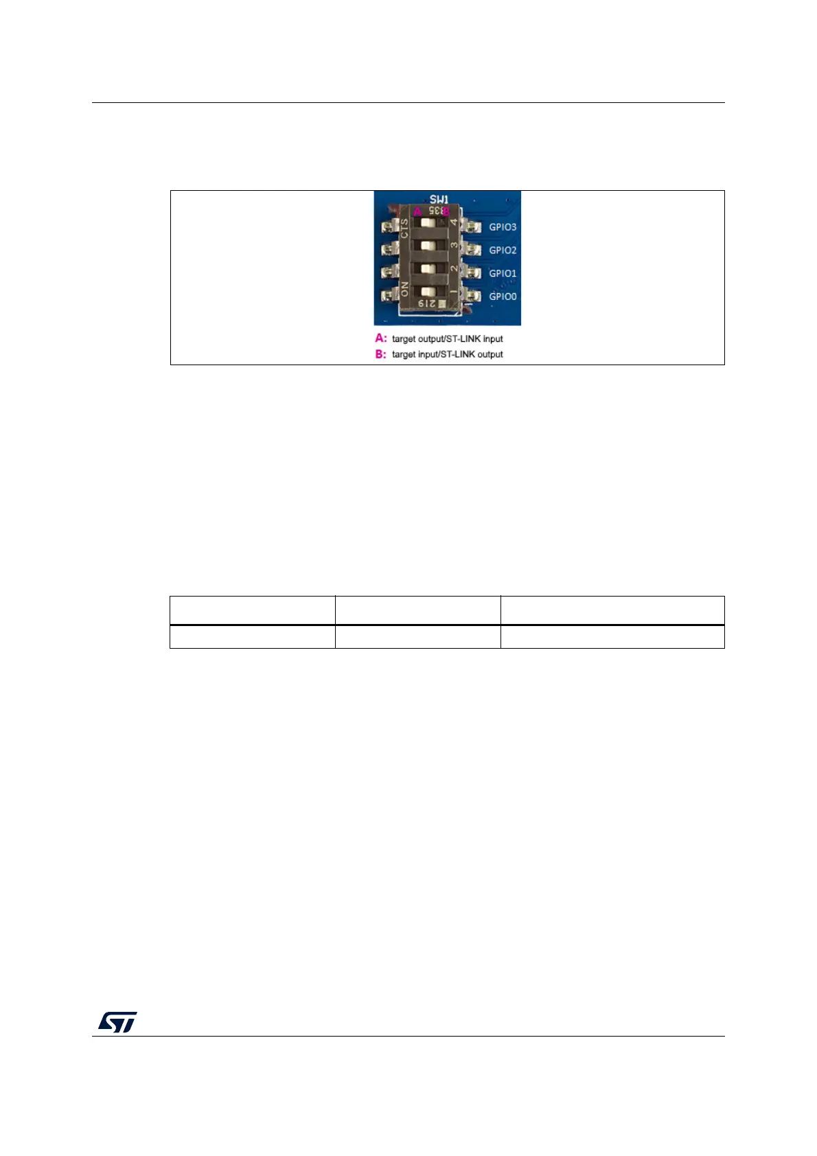
changed for each GPIO independently into the target input/ST-LINK output direction by
moving the corresponding selector on the ‘1’, ‘2’, ‘3’, or ‘4’ side of SW1. Refer to
Figure 18.
Figure 18. B-STLINK-VOLT
12.4 Jumper configuration
Caution: Always remove the JP1 jumper from the STLINK-V3SET main module (MB1441) before
stacking the B-STLINK-VOLT board (MB1598). This jumper can be used on the MB1598
board to provide the return JTAG clock required for correct JTAG operations. If the JTAG
clock loopback is not done at the B-STLINK-VOLT board level through JP1, it must be done
externally between pin 6 and pin 9 of CN1.
12.5 Target voltage connection
The target voltage must always be provided to the board for proper operation (input for
B-STLINK-VOLT). It must be provided to pin 3 of the STDC14 connector (CN1), either
directly on MB1598 or through the MB1440 adapter board. In case of use with the MB1440
adapter board, the target voltage can be provided either through the pin3 of CN1, pin1 of
CN2, pin1 of CN6, or pin2 and pin3 of JP10 of the MB1440 board. The expected range is
1.65
V - 3.3 V.
Table 18. MB1598 jumper configuration
Jumper State Description
JP1 ON JTAG clock loopback done on board
 Loading...