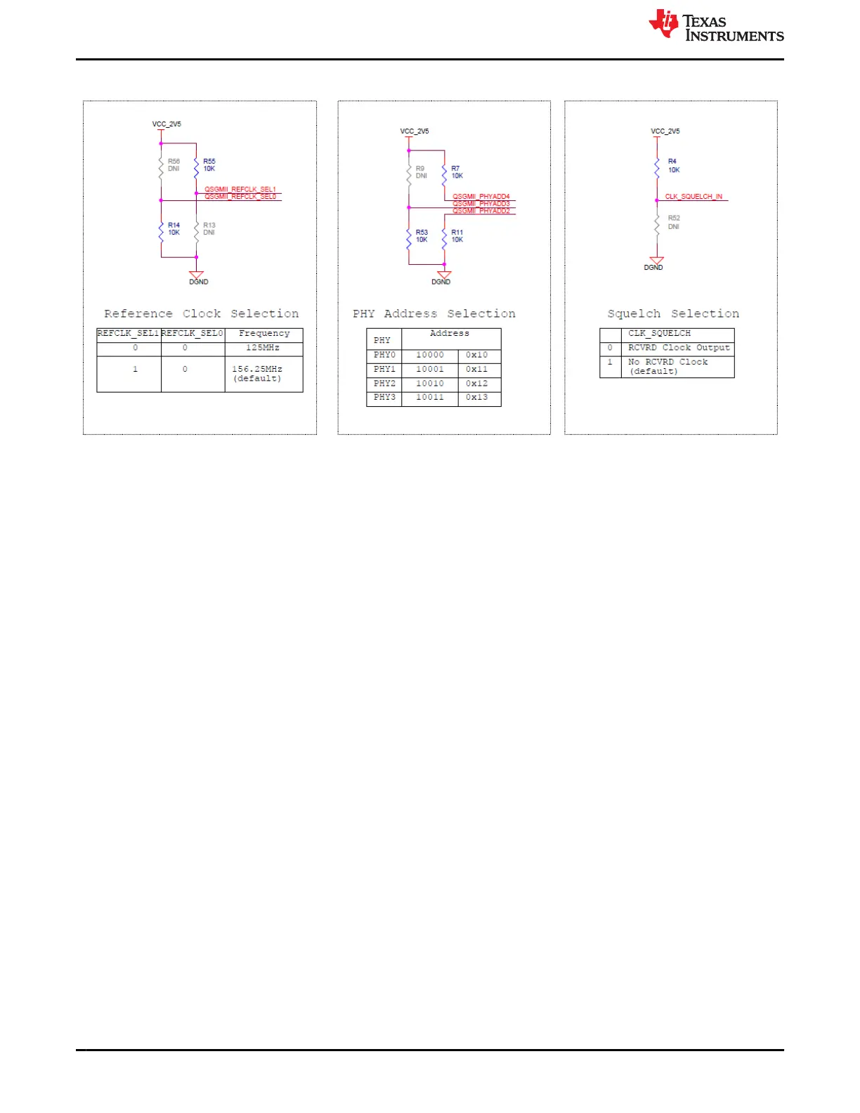
The resistor strapping options are shown in Figure 4-18.
Figure 4-18. QSGMII Ethernet PHY Settings
4.11 PCIe Interface
The Common processor board is supporting two X4 lane (One for x1L and One for x2L interface), PCIe
connector to accept PCIe form factor daughter card and support PCIe Gen4 operation. The EVM also supports
the PCIe M.2 socket to interface the M keyed PCIe M.2 form factor modules, which are not included in the EVM
kit.
4.11.1 X1 Lane PCIe Interface
The x1 lane PCIe interface includes one x4 lane PCIe connector of part number Amphenol 10142333-10111MLF,
which supports PCIe Gen4 operation. The pin-out of the connector follows PCIe standard.
The SERDES0 port of J7 SoC is connected to x1 lane PCIe socket for data transfer. PCIe0, USB0_SS and
SGMII1, 2 interfaces are pinmuxed with this SERDES0 port.
I2C0 from SoC is used for control purpose and is connected to SMBUS on the connector. I2C0 port is connected
to both x1 lane and x2 lane PCIe connectors using a Mux TCA9543APWR.
J721E EVM Hardware Architecture www.ti.com
52 Jacinto7 J721E/DRA829/TDA4VM Evaluation Module (EVM) SPRUIS4D – MAY 2020 – REVISED MARCH 2022
Submit Document Feedback
Copyright © 2022 Texas Instruments Incorporated
 Loading...