Home
Texas Instruments
Motherboard
J721E
Texas Instruments J721E User Manual
4
of 1
of 1 rating
84 pages
Give review
Manual
Specs
To Next Page
To Next Page
To Previous Page
To Previous Page
Loading...
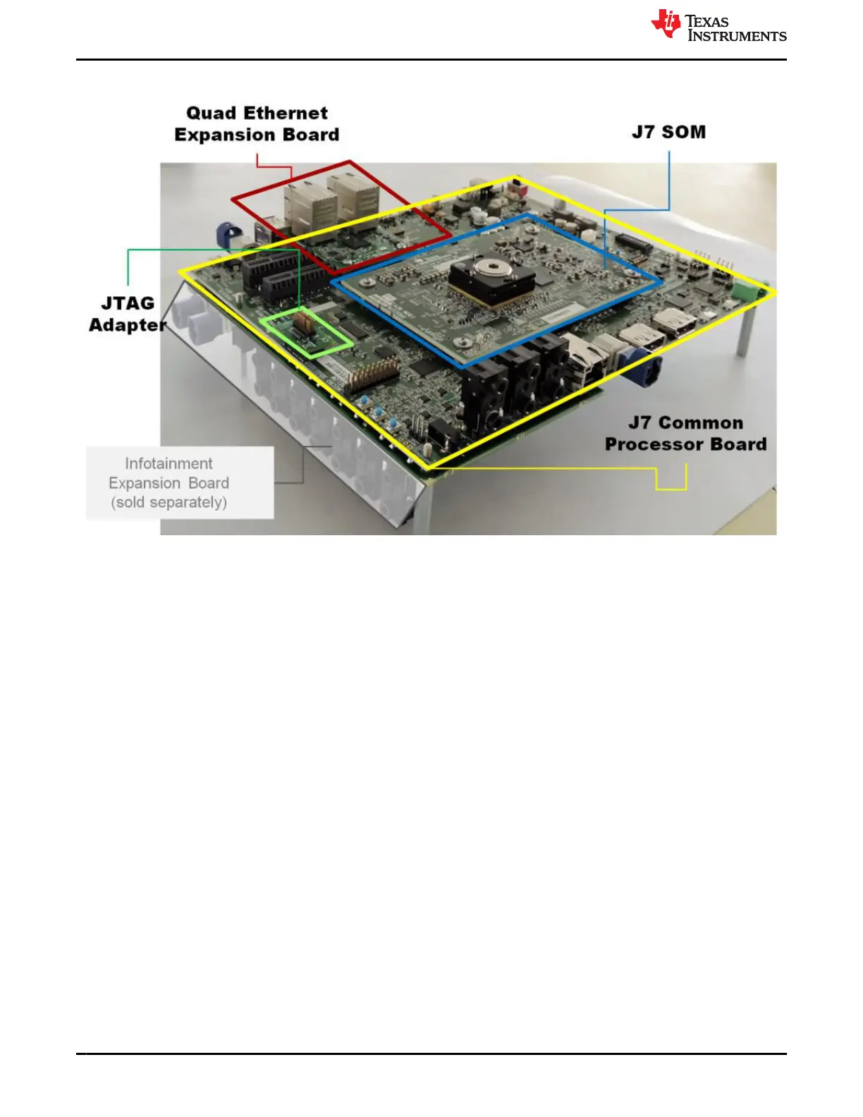
2.1 J721E EVM Board Identification
Figure 2-3. J721E EVM Board Identification (SOM, CPB, QP Ethernet)
J721E EVM Overview
www
.ti.com
8
Jacinto7 J721E/DRA829/TDA4VM Evaluation Module (EVM)
SPRUIS4D – MA
Y 2020 – REVISED MARCH 2022
Submit Document Feedback
Copyright © 2022 T
exas Instruments Incorporated
7
9
Table of Contents
Table of Contents
1
Introduction
4
Key Features
4
Thermal Compliance
5
Figure 1-1. Thermal Caution
5
REACH Compliance
6
EMC, EMI, and ESD Compliance
6
J721E EVM Overview
6
Figure 2-1. J721E EVM Board
6
Table 1-1. REACH Compliance
6
Figure 2-2. System Architecture Interface
7
J721E EVM Board Identification
8
Figure 2-3. J721E EVM Board Identification (SOM, CPB, QP Ethernet)
8
J721E SOM Component Identification
9
Figure 2-4. J721E SOM Component Identification
9
Jacinto7 Common Processor Components Identification
10
Figure 2-5. Jacinto7 Common Processor Component Identification
10
Quad Ethernet Components Identification
11
Figure 2-6. Quad Ethernet Component Identification
11
EVM User Setup/Configuration
12
Power Requirements
12
Figure 3-1. Connector Used for Power Input
12
Table 3-1. Recommended External Power Supply
12
Power on Switch and Power Leds
13
Figure 3-2. Power ON/OFF Switch
13
Figure 3-3. Power On/Fault Leds
14
Table 3-2. Power LED Status
14
Figure 3-4. Power Status Leds
15
Table 3-3. Power Leds
15
Table 3-4. Power Test Points
16
EVM Reset/Interrupt Push Buttons
17
Figure 3-5. EVM Push Buttons
17
Table 3-5. EVM Push Buttons
17
EVM DIP Switches
18
Figure 3-6. EVM Configuration DIP Switch
18
Table 3-6. EVM Configuration Switch Function
19
Table 3-7. EVM Configuration Switch Function
20
Figure 3-7. BOOT Switches Provided on the Processor Card
21
Table 3-8. Wakup Boot Mode Switch (SW9)
21
Table 3-9. Main Boot Mode Switch (SW8)
21
EVM UART/COM Port Mapping
22
Table 3-10. UART Port Mapping
22
JTAG Emulation
23
Figure 3-8. JTAG Mux
23
Table 3-11. JTAG 1:2 Mux Selection
23
Table 3-12. TI 60 Pin Connector (J16) Pinout
24
Table 3-13. Cti20 Pin Connector (J1-Refer PROC081E2 SCH) Pinout
25
Table 3-14. TI14 Pin Connector (J2-Refer PROC081E2 SCH) Pinout
25
J721E EVM Hardware Architecture
26
J721E EVM Hardware Top Level Diagram
26
Figure 4-1. J721E EVM Functional Block Diagram
26
Figure 4-2. Quad Port Ethernet Expansion Functional Block Diagram
27
J721E EVM Interface Mapping
28
Table 4-1. J721E EVM Interface Mapping
28
I2C Address Mapping
29
Table 4-2. J721E EVM I2C Table
29
GPIO Mapping
30
Table 4-3. J721E Soc - GPIO Mapping Table
30
Power Supply
31
Figure 4-3. J721E SOM Power Distribution Block Diagram
31
Figure 4-4. Power on Sequencing
32
Figure 4-5. Voltage Supervisor Circuit
33
Figure 4-6. LPDDR4 IO Voltage Selection Circuit
34
Table 4-4. DDR I/O Voltage Selection
34
Table 4-5. J721E Soc S2R Logic Flow
35
Table 4-6. J721E Soc S2R Logic Flow
35
Table 4-7. INA Devices I2C Slave Address
36
Table 4-8. External Power Monitor Header Pinouts
37
Reset
38
Figure 4-7. EVM Reset Architecture
38
Clock
39
Figure 4-8. EVM Clock Architecture
39
Figure 4-9. J721E Soc Primary Clock
40
Table 4-9. Processor's Secondary/Serdes Ref Clock
41
Table 4-10. EVM Peripheral Ref Clock
41
Memory Interfaces
42
Figure 4-10. J721E Som LPDDR4
42
Figure 4-11. J721E Som OSPI and Hyper Flash
43
Figure 4-12. UFS Memory Block Diagram
44
Figure 4-13. Emmc Memory Block Diagram
45
Figure 4-14. Micro-SD Card Block Diagram
46
Table 4-11. Board ID Memory Header Information
47
MCU Ethernet Interface
48
Figure 4-15. MCU Gigabit Ethernet Block
48
Figure 4-16. MCU Ethernet PHY Settings
49
QSGMII Ethernet Interface
50
Table 4-12. Clock Source Selection
50
Figure 4-17. Quad-SGMII Board I2C
51
Pcie Interface
52
Figure 4-18. QSGMII Ethernet PHY Settings
52
Figure 4-19. Pcie Interface for SERDES0
53
Figure 4-20. Pcie SMBUS Block Diagram
53
Figure 4-21. 1L-Pcie Root Complex/Endpoint Selection Circuit
54
Table 4-13. Reference Clock Selection for Pcie Host Operation
54
Table 4-14. Reference Clock Selection for Pcie Endpoint Operation
54
Figure 4-22. USB2.0 Header Connection
55
Table 4-15. Resistors for Selecting Pcie Card Host or Device
55
Figure 4-23. Pcie Interface for SERDES1
56
Figure 4-24. 2L-Pcie Root Complex/Endpoint Selection Circuit
56
Table 4-16. Reference Clock Selection for Pcie Host Operation
57
Table 4-17. Reference Clock Selection for Pcie Endpoint Operation
57
Table 4-18. Resistors for Selecting Pcie Card Host or Device Operation
57
USB Interface
58
Figure 4-25. Pcie Interface for SERDES2
58
Figure 4-26. USB3.1 Type C Interface
59
Figure 4-27. Type C Power Delivery Current Settings
59
Figure 4-28. USB Hub Reference Clock Circuit
60
Figure 4-29. USB Hub Settings Circuit
60
Figure 4-30. USB1 ID Setting for HUB
60
CAN Interface
61
Figure 4-31. MCU CAN0 Interface
61
Figure 4-32. CAN Wake Push Button
62
Figure 4-33. CAN Header Connections to Db9/Test Instrument
63
FPD Interface (Audio Deserializer)
64
Figure 4-34. FPD-Link UB926 ID Setting Circuit
64
Figure 4-35. FPD-Link UB926 Mode Selection Circuit
64
FPD Panel Interface (DSI Video Serializer)
65
Figure 4-36. FPD-Link UB941A Device Settings Circuit
65
Table 4-19. FPD Audio Deserializer HSD Connector Pinout
65
Table 4-20. DSI to FPD Serializer HSD Connector Pinout
65
Display Serial Interface (DSI) FPC
66
Audio Interface
66
Table 4-21. MCASP/TRACE - 1:3 MUX: Truth Table
66
Table 4-22. Config Table
66
Figure 4-37. Audio Port Interface Assignment
67
Display Port Interface
68
MLB Interface
68
Figure 4-38. Display Port Block Diagram
68
Figure 4-39. MLB Interface Connector
69
Table 4-23. MLB Header Pinout
69
I3C Interface
70
ADC Interface
70
Figure 4-40. ADC Interface Connector
70
Table 4-24. MCU I3C Header J33 Pinout
70
Table 4-25. MAIN I3C Header J32
70
RTC Interface
71
Figure 4-41. RTC Block Diagram
71
Table 4-26. ADC Header J23
71
Apple Authentication Header
72
Figure 4-42. Apple Authentication Block Diagram
72
Table 4-27. APPLE AUTH Header J9
72
EVM Expansion Connectors
73
Figure 4-43. Expansion Board Interface Connectors
73
Table 4-28. APPLE AUTH Footprint U108 Pinout
73
Table 4-29. EVM Expansion Connector J46
74
Table 4-30. EVM Expansion Connector J51
76
ENET Expansion Connector
77
Table 4-31. ENET Expansion Board Power Test Points
77
Figure 4-44. CDCI I2C Isolation Circuit
78
Table 4-32. ENET Expansion Connector J10 Pinout
79
Table 4-33. CSI Expansion Connector J52 Pinout
82
Table 4-34. CSI Expansion Connector J48 Pinout
82
4
Based on 1 rating
Ask a question
Give review
Questions and Answers:
Need help?
Do you have a question about the Texas Instruments J721E and is the answer not in the manual?
Ask a question
Texas Instruments J721E Specifications
General
Brand
Texas Instruments
Model
J721E
Category
Motherboard
Language
English
Related product manuals
Texas Instruments INA228
32 pages
Texas Instruments M-LVDS
32 pages
Texas Instruments LMK04826
54 pages
Texas Instruments LMK04828
113 pages
Texas Instruments BQ79600-Q1
25 pages
Texas Instruments TM4C Series
36 pages
Texas Instruments Tiva TM4C1294
34 pages
Texas Instruments mmWaveICBoost
80 pages
Texas Instruments EK-TM4C123GXL
27 pages
LMX2615EVM-CVAL
21 pages
DS90UB954-Q1EVM
55 pages
C2000 F28003x Series
30 pages
 Loading...