SARA-R5 series - System integration manual
UBX-19041356 - R04 System description Page 10 of 118
C1-Public
Base-Band and Power Management section
The Base-Band and Power Management section, based on the u-blox UBX-R5 cellular chipset, is
composed of the following main elements:
• On-chip modem processor, vector signal processor, with dedicated hardware assistance for signal
processing and system timing
• On-chip modem processor, with interfaces control functions
• On-chip voltage regulators to derive all the internal or external (V_SIM, V_INT) supply voltages
from the module supply input VCC
• On-chip cryptographic hardware acceleration with Root of Trust
• On-chip memory system, including pSRAM and secure boot ROM
• Dedicated flash memory IC
• Dedicated secure element
• 32.768 kHz crystal oscillator to provide the clock reference in the low power idle mode, which can
be enabled using the +UPSV AT command, and in the PSM deep-sleep mode, which can be enabled
using the +CPSMS in addition to the +UPSV AT command
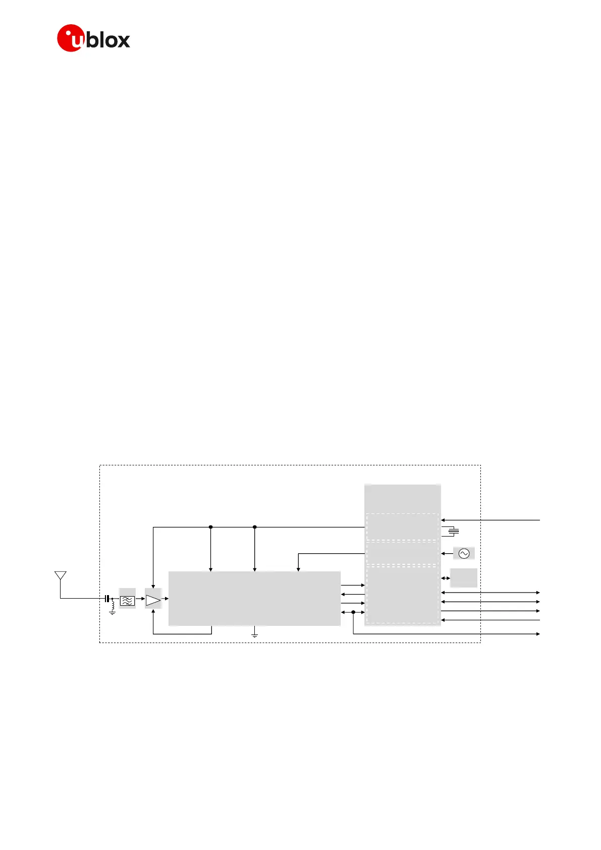
GNSS section
The GNSS section, based on the u-blox UBX-M8 GNSS chipset, is composed of the following main
elements illustrated in Figure 4:
• u-blox UBX-M8030 concurrent GNSS chipset with SPG 3.01 firmware version
• Dedicated SAW filter
• Additional Low Noise Amplifier (LNA)
• 26 MHz Temperature-Controlled Crystal Oscillator (TCXO) generating the reference clock signal
for the cellular RF transceiver, the Base-Band system and the GNSS system

 Loading...


