ML605 Hardware User Guide www.xilinx.com 25
UG534 (v1.9) February 26, 2019
Detailed Description
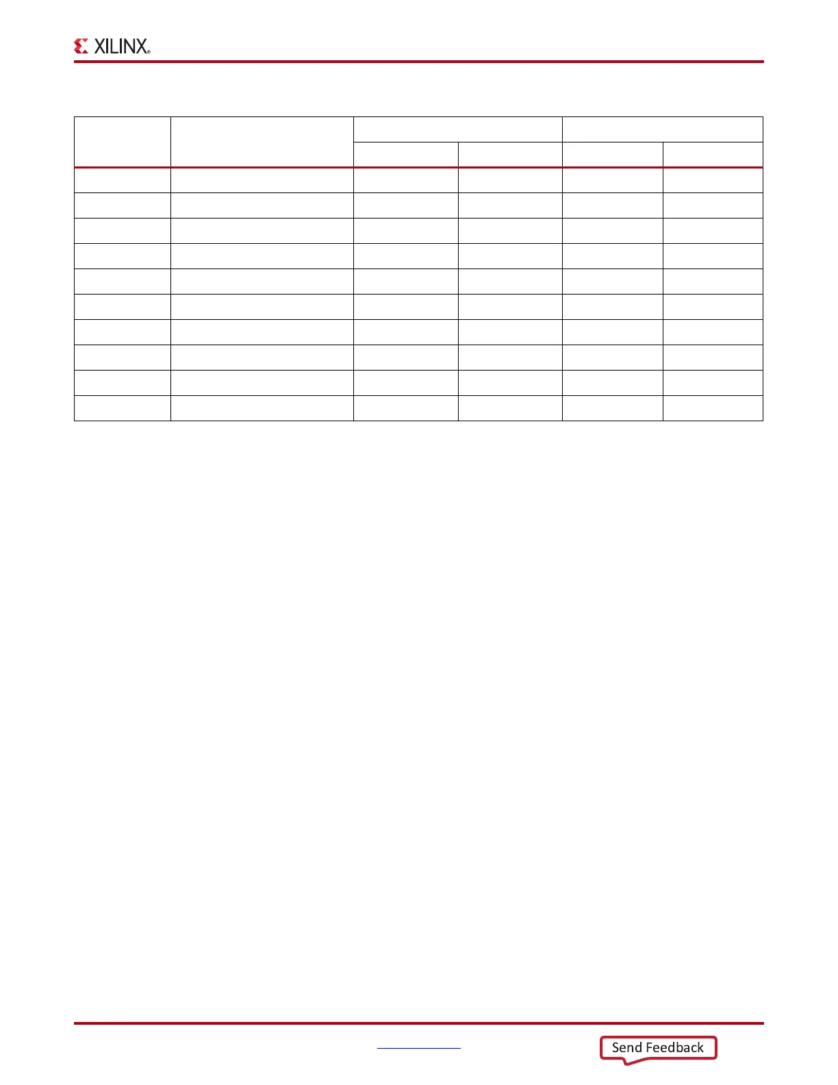
M23 FLASH_D15 54 DQ15 E7 DQ15
J26 FLASH_WAIT 56 WAIT NA
(1)
NA
(1)
AF23 FPGA_FWE_B 14 /WE G8 /W
AA24 FPGA_FOE_B 32 /OE F8 /G
K8 FPGA_CCLK NA
(1)
NA
(1)
F1 K
AC23 PLATFLASH_L_B NA
(1)
NA
(1)
H1 /L
Y24 FPGA_FCS_B
(2)
NA
(1)
NA
(1)
NA
(1)
NA
(1)
NA
(1)
PLATFLASH_FCS_B
(3)
NA
(1)
NA
(1)
B4 /E
NA
(1)
FLASH_CE_B
(4)
30 /OE NA
(1)
NA
(1)
Notes:
1. Not Applicable
2. FPGA control flash memory select signal connected to pin U10.3
3. Platform Flash select signal connected to pin U10.6
4. BPI Flash select signal connected to pin U10.4
Table 1-5: Platform Flash and BPI Flash Connections (Cont’d)
U1 FPGA Pin Schematic Net Name
U4 BPI Flash U27 Platform Flash
Pin Number Pin Name Pin Number Pin Name

 Loading...


