SP605 Hardware User Guide www.xilinx.com 25
UG526 (v1.9) February 14, 2019
Detailed Description
See the System ACE CF product page, System ACE file generation information, and the
System ACE CompactFlash Solution Data Sheet (DS080) [Ref 5] for more information.
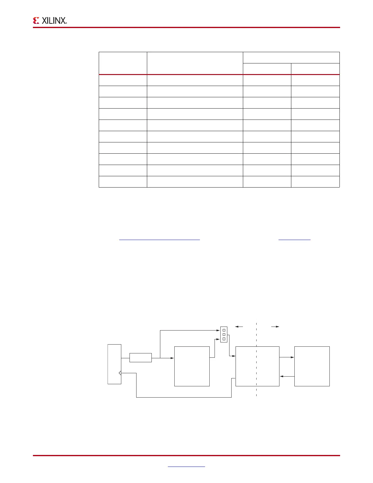
6. USB JTAG
JTAG configuration is provided through onboard USB-to-JTAG configuration logic where
a computer host accesses the SP605 JTAG chain through a Type-A (computer host side) to
Type-Mini-B (SP605 side) USB cable. The JTAG chain of the board is illustrated in
Figure 1-6. JTAG configuration is allowable at any time under any mode pin setting. JTAG
initiated configuration takes priority over the mode pin settings.
FMC bypass jumper J19 must be connected between pins 1-2 (bypass) to enable JTAG
access to the FPGA on the basic SP605 board (without FMC expansion modules installed),
AA1 SYSACE_MPBRDY 39 MPBRDY
W4 SYSACE_MPCE 42 MPCE
AA2 SYSACE_MPIRQ 41 MPIRQ
T6 SYSACE_MPOE 77 MPOE
T5 SYSACE_MPWE 76 MPWE
G17 SYSACE_CFGTDI 81 CFGTDI
A21 FPGA_TCK 80 CFGTCK
E18 FPGA_TDI 82 CFGTDO
D20 FPGA_TMS 85 CFGTMS
N19 CLK_33MHZ_SYSACE(2) 93 CLK
Notes:
1. U17 System ACE CF controller 3.3V signals as named are wired to a set of TXB0108 3.3V-to-1.5V level
shifters. The nets between the 1.5V side of the level shifters and the U1 FPGA have the same names
with _LS appended.
2. The System ACE CF clock is sourced from U29 32.000MHz oscillator.
Table 1-8: System ACE CF Connections (Cont’d)
U1 FPGA Pin Schematic Net Name
(1)
U17 XCCACETQ144I
Pin Number Pin Name
X-Ref Target - Figure 1-6
Figure 1-6: JTAG Chain Diagram
FMC LPC
TDO
U1
FPGA
TDITSTTDI CFGTDO
CFGTDI
TSTTDO TDO
System ACE CF
3.3V 2.5V
TDI
Buffer
USB Header
J4
J2
J19
U17
UG526_06_092409

 Loading...


