SP605 Hardware User Guide www.xilinx.com 33
UG526 (v1.9) February 14, 2019
Detailed Description
10. SFP Module Connector
The board contains a small form-factor pluggable (SFP) connector and cage assembly that
accepts SFP modules. The SFP interface is connected to MGT Bank 123 on the FPGA. The
SFP module serial ID interface is connected to the “SFP” IIC bus (see 14. IIC Bus for more
information). The control and status signals for the SFP module are connected to jumpers
and test points as described in Table 1-12. The SFP module connections are shown in
Table 1-13.
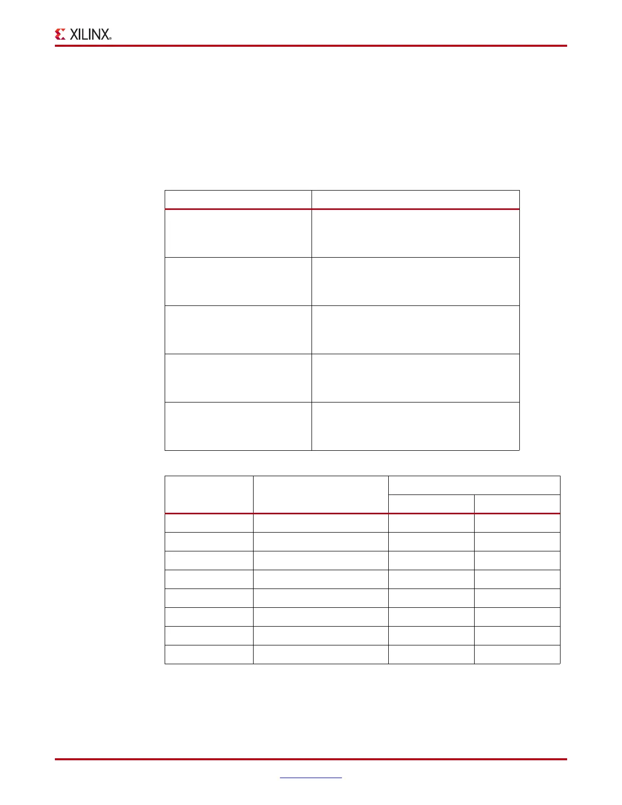
Table 1-12: SFP Module Control and Status
SFP Control/Status Signal Board Connection
SFP_TX_FAULT
Test Point J15
High = Fault
Low = Normal Operation
SFP_TX_DISABLE
Jumper J44
On = SFP Enabled
Off = SFP Disabled
SFP_MOD_DETECT
Test Point J16
High = Module Not Present
Low = Module Present
SFP_RT_SEL
Jumper J22
Jumper Pins 1-2 = Full Bandwidth
Jumper Pins 2-3 = Reduced Bandwidth
SFP_LOS
Test Point J14
High = Loss of Receiver Signal
Low = Normal Operation
Table 1-13: SFP Module Connections
U1 FPGA Pin Schematic Net Name
P2 SFP Module Connector
Pin Number Pin Name
D13 SFP_RX_P 13 RDP
C13 SFP_RX_N 12 RDN
B14 SFP_TX_P 18 TDP
A14 SFP_TX_N 19 TDN
T17 SFP_LOS 8 LOS
Y8 SFP_TX_DISABLE_FPGA 3 TX_DISABLE
A12 SFPCLK_QO_N
(1)
U47.6
(2)
-
B12 SFPCLK_QO_P
(1)
U47.7
(2)
-
Notes:
1. The 125MHz SFP clock is sourced by clock driver U47.
2. Not P2 SFP module pins.

 Loading...


