38 www.xilinx.com SP605 Hardware User Guide
UG526 (v1.9) February 14, 2019
Chapter 1: SP605 Evaluation Board
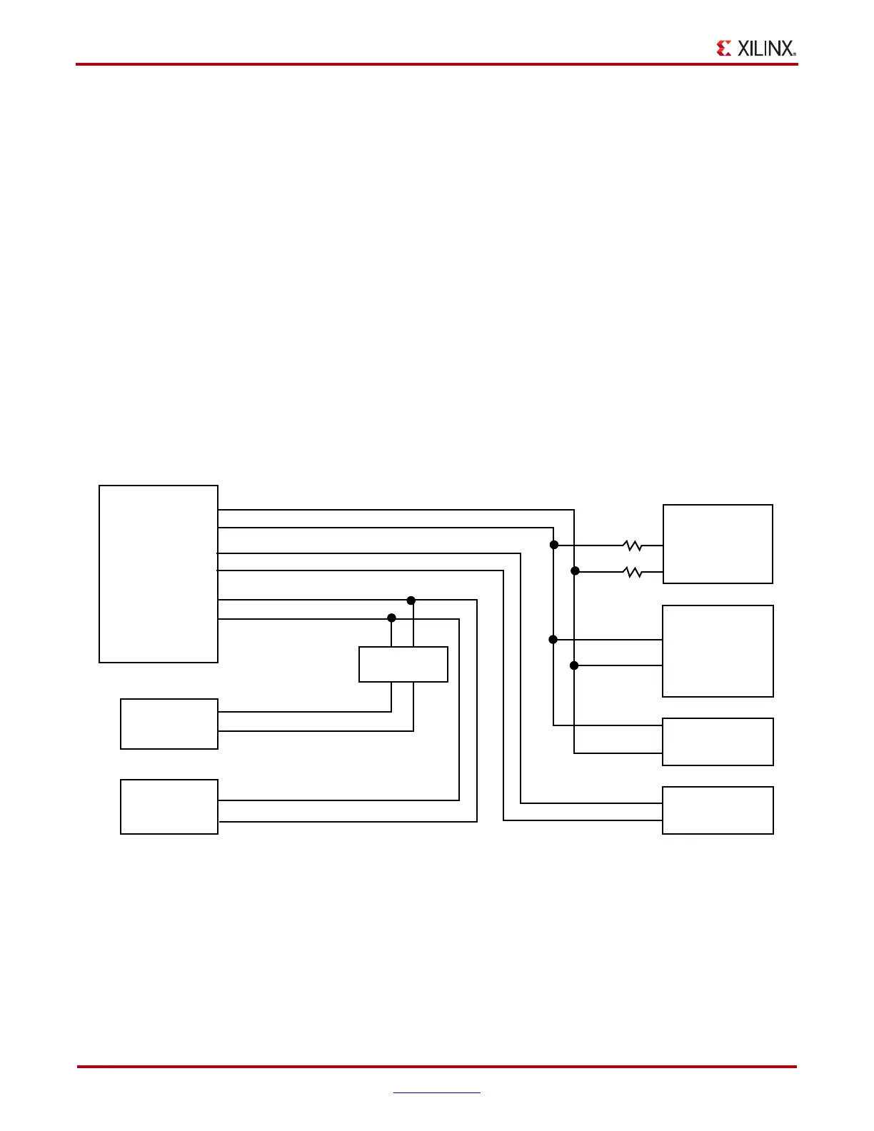
14. IIC Bus
The SP605 implements three IIC bus interfaces at the FPGA.
The MAIN IIC bus hosts four items:
• FPGA U1 Bank 1 “MAIN” IIC interface
•8-Kb NV Memory U4
• FMC LPC connector J2
• 2-Pin External Access Header J45
The DVI IIC bus hosts two items:
• FPGA U1 Bank 2 DVI IIC interface
• DVI Codec U31 and DVI connector P3
The SFP IIC bus hosts two items:
• FPGA U1 Bank 0 SFP IIC interface
• SFP module connector P2
The SP605 IIC bus topology is shown in Figure 1-11.
X-Ref Target - Figure 1-11
Figure 1-11: IIC Bus Topology
U1
P3
U31
BANK 1
IIC_SDA_MAIN
IIC_SCL_MAIN
IIC_SDA_SFP
IIC_SCL_SFP
IIC_SDA_DVI
IIC_SCL_DVI
U4
J2
IIC_CLK_DVI_F
ST MICRO
M24C08-WDW6TP
FMC LPC
Column C
2 Kb EEPROM on
any FMC LPC
Mezzanine Card
P2
SFP Module
Connector
IIC_SDA_DVI_F
BANK 0
BANK 2
FPGA IIC
INTERFACE
Addr: 0b1010000
Addr: 0b1110110
Addr: 0b1010100
through
0b1010111
Addr: 0b1010010
Addr: 0b1010000
J45
2-Pin External
Access Header
DVI Connector
DVI CODEC
CHRONTEL
CH730C-TF
LEVEL
SHIFTER
UG526_11_092609

 Loading...


