ZCU104 Board User Guide 34
UG1267 (v1.1) October 9, 2018 www.xilinx.com
Chapter 3: Board Component Descriptions
Quad SPI Flash Memory (MIO 0–5)
[Figure 2-1, callout 4]
The Micron MT25QU512ABB8ESF serial NOR flash Quad SPI flash memory can hold the boot
image for the MPSoC system. This interface is used to support QSPI32 boot mode as
defined in the Zynq UltraScale+ MPSoC Technical Reference Manual (UG1085) [Ref 2].
The Quad SPI flash memory (U119) is located on the bottom of the board, and provides
512 Mb of non-volatile storage that can be used for configuration and data storage.
• Part number: MT25QU512ABB8ESF-0SIT (Micron)
• Supply voltage: 1.8V
• Datapath width: 4 bits
• Data rate: Various depending on single, dual, or quad mode
The connections between the SPI flash memory and the XCZU7EV MPSoC are listed in
Table 3-6.
M I O 9 C 2 6 N o t Co n n e c t e d N C M I O 3 5 C3 1 N o t C o n n e ct e d N C M I O 6 1 H3 4 M I O6 1 _ U S B _D A T A 5 _R U S B 0
M I O 8 D 2 6 N o t Co n n e c t e d N C M I O 3 4 B 3 4 N o t C o n n e c te d N C M I O 60 H 3 3 M IO 6 0 _ U S B_ D A T A 4_ R U S B 0
M I O 7 B 2 5 N o t C on n e c t e d N C M IO 3 3 B 3 3 N o t C o n n ec t e d N C M I O 5 9 H 3 2 M I O 5 9 _U S B _ D A TA 3 _ R U S B0
M I O 6 A 2 6 N o t C o nn e c t e d N C M I O3 2 B 3 1 N o t C o n n e ct e d N C M I O 5 8 H 3 1 M I O 5 8_ U S B _ ST P _ R U S B0
M I O 5 D 2 5 M I O 5 _ Q S P I _ L W R _ C S _ B Q S P I M I O 3 1 B 3 0 N o t C o n n e c t e d N C M I O 5 7 H 2 9 M I O 5 7 _ U S B _ D A T A 1 _ R U S B 0
MIO4 A25 MIO4_QSPI_LWR_DQ0 QSPI MIO30 A33 MIO30_DP_AUX_IN DPAUX MIO56 G34 MIO56_USB_DATA0_R USB0
MIO3 E25 MIO3_QSPI_LWR_DQ3 QSPI MIO29 A32 MIO29_DP_OE DPAUX MIO55 G33 MIO55_USB_NXT USB0
MIO2 B24 MIO2_QSPI_LWR_DQ2 QSPI MIO28 A31 MIO28_DP_HPD DPAUX MIO54 G31 MIO54_USB_DATA2_R USB0
MIO1 C24 MIO1_QSPI_LWR_DQ1 QSPI MIO27 A30 MIO27_DP_AUX_OUT DPAUX MIO53 G30 MIO53_USB_DIR USB0
MIO0 A24 MIO0_QSPI_LWR_CLK QSPI MIO26 A29 Not Connected NC MIO52 G29 MIO52_USB_CLK USB0
Table 3-5: MIO Connections (Cont’d)
MIO
[25:0]
Bank 500
ZU7EV
U1
Pin
No.
Schematic Net Name Type
MI
[51:26]
Bank
501
ZU7EV
U1
Pin
No.
Schematic Net Name Type
MIO
[77:52]
Bank 502
ZU7EV
U1
Pin
No.
Schematic Net Name Type
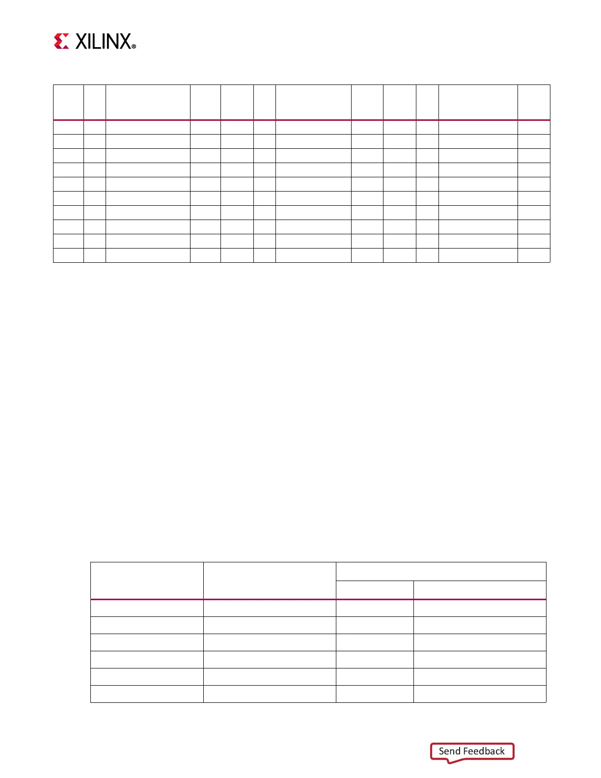
Table 3-6: Quad SPI Flash Memory Component Connections to MPSoC U1
XCZU7EV (U1) Pin Net Name
Quad SPI U119 (LWR), U120 (UPR)
Pin # Pin Name
A25 MIO4_QSPI_LWR_DQ0 15 DQ0
C24 MIO1_QSPI_LWR_DQ1 8 DQ1
B24 MIO2_QSPI_LWR_DQ2 9 DQ2_WP_B
E25 MIO3_QSPI_LWR_DQ3 1 DQ3_RST_HOLD_B
A24 MIO0_QSPI_LWR_CLK 16 C
D25 MIO5_QSPI_LWR_CS_B 7 S_B

 Loading...


