ZCU104 Board User Guide 61
UG1267 (v1.1) October 9, 2018 www.xilinx.com
Chapter 3: Board Component Descriptions
HDMI Clock Recovery
[Figure 2-1, callout 29]
The ZCU104 board includes an IDT 8T49N241 jitter attenuator U181. The 8T49N241 has one
fractional feedback phase-locked loop (PLL) that can be used as a jitter attenuator and
frequency translator.
The FPGA can output the RX recovered clock to a differential I/O pair on I/O bank 67
(HDMI_REC_CLOCK_P, pin G14 and HDMI_REC_CLOCK_N, pin F13) for jitter attenuation. The
jitter attenuated clock (HDMI_SI5324_OUT_C_P (U181 pin 22), HDMI_SI5324_OUT_C_N
(U081 pin 39) is then routed as a series capacitor coupled reference clock to GTH Quad 227
inputs MGTREFCLK0P (U1 pin T8) and MGTREFCLK0N (U1 pin T7).
The 8T49N241 is used to generate the reference clock for the HDMI transmitter subsystem.
When the HDMI transmitter is used in standalone mode, the 8T49N241 operates in
free-running mode and uses an external oscillator as the reference. When the HDMI
transmitter is used in pass-through mode, the 8T49N241 generates a jitter attenuated
reference clock to drive the HDMI transmitter subsystem with a phase-aligned version of
the HDMI Rx subsystem HMDI Rx TMDS clock, so that they are phase aligned. The
8T49N241 is controlled by an I2C interface connected to the FPGA. Enabling the jitter
attenuation feature requires additional user programming through the FPGA connected
HDMI_CTL I2C bus. The jitter attenuated clock circuit is shown in Figure 3-19.
IMPORTANT: The IDT 8T49N241 pin 31 reset net HDMI_8T49N241_RST must be driven High to enable
the device. U181 pin 31 net HDMI_8T49N241_RST is connected to FPGA U1 bank 87 pin M12.
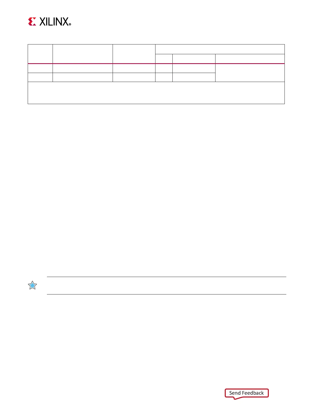
D2 HDMI_RX_SNK_SCL LVCMOS33 1 SCL_A
TPD12S016RK (U102)
E2 HDMI_RX_SNK_SDA LVCMOS33 1 SDA_A
Notes:
1. U1 MGT (I/O standards do not apply).
2. TMDS181IRG (U19), SN65DP159 (U94), M24C64-W (U109), and SI5324C (U108).
Table 3-22: HDMI Connections to MPSoC U1 (Cont’d)
XCZU7EV
(U1) Pin
Schematic Net Name I/O Standard
Connected Component
Pin Name Device

 Loading...


