ZCU104 Board User Guide 50
UG1267 (v1.1) October 9, 2018 www.xilinx.com
Chapter 3: Board Component Descriptions
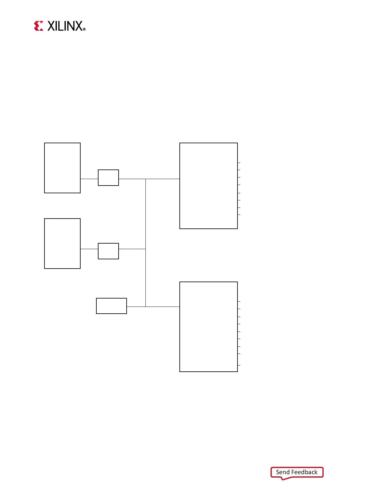
I2C1 (MIO 16-17)
[Figure 2-1, callouts 12 and 13]
The I2C1 interface provides access to I2C peripherals through I2C switch TCA9548A U34. A
TCA6416A port expander U97 is also attached to the I2C1 bus. The I2C1 PS-side bank 500
connection is shared with PL-side bank 87. Figure 3-12 shows a high-level view of the I2C1
bus connectivity represented in Table 3-16 and Table 3-17. TCA9548A U34 is set to 0x74
and the TCA6416A is set to 0x20 .
X-Ref Target - Figure 3-12
Figure 3-12: I2C1 Bus Topology
BANK 500
U1
MIO17(C29)
MIO16(A28)
PS I2C1
BANK 87
U1
PL I2C1
P12/N12
TCA9548A
U34
SC0/SC0
SD1/SC1
SDA/
SCL
L/S
U136
IIC_EEPROM_SDA/SCL
8T49N287_SDA/SCL
SC2/SC2
SD3/SC3
IRPS5401_SDA/SCL
VCC12_INA226_SDA/SCL
SC4/SC4
SD5/SC5
NOT CONNECTED
FMC_LPC_IIC_SDA/SCL
SC6/SC6
SD7/SC7
NOT CONNECTED
DDR4_SODIMM_SDA/SCL
0x34
0x7C
0x##
0x51
TCA6416A
U97
P00
P01
SDA/
SCL
IRPS5401_ALERT_B
HDMI_8T49N241_INT_ALM
P02
P03
MAX6643_OT_B
MAX6643_FANFAIL_B
P04
P05
VCC12_INA226_ALERT
IIC_MUX_RESET_B
P06
P07
GEM3_EXP_RESET_B
FMC_LPC_PRSNT_M2C_B
P10-P17
NOT CONNECTED
L/S
U45
SDA 7,8
SCL 5,6
2x6 Male Pin Hdr.
0x74
0x20
I2C1_SDA/SCL
0x7C
PMIC1 0X13
PMIC2 0X14
{
0x40
J160
X20117-021218

 Loading...


