ZCU104 Board User Guide 44
UG1267 (v1.1) October 9, 2018 www.xilinx.com
Chapter 3: Board Component Descriptions
Clock Generation
The ZCU104 board provides an IDT8T49N287 FemtoClock® NG octal universal frequency
translator (U182) clock generator. Table 3-12 lists the frequency for each clock.
Table 3-13 lists the connectivity for each clock.
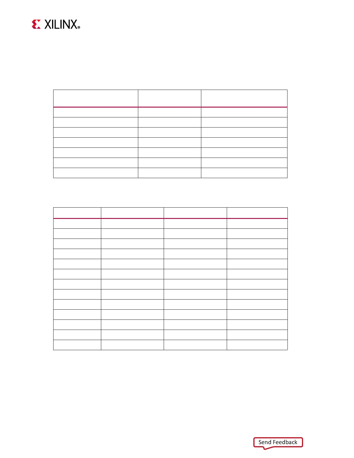
Table 3-12: Clock Sources
Clock (Net) Name Frequency
IDT8T49N287 U182
Clock Output
HDMI_DRU_CLOCK 156.25 MHz Q0
PS_REF_CLK 33.33 MHz Q1
GTR_REF_CLK_USB3 26 MHz Q2
GTR_REF_CLK_DP 27 MHz Q3
CLK_300_P 300 MHz Q4
GTR_REF_CLK_SATA 125 MHz Q5
CLK_125 125 MHz Q6
Table 3-13: Clock Connections, Source to XCZU7EV MPSoC
Clock Source Pin Net Name I/O Standard XCZU7EV (U1) Pin
U182.48 HDMI_DRU_CLOCK_P
(2)
U10
U182.47 HDMI_DRU_CLOCK_N
(2)
U9
U182.44 PS_REF_CLK LVCMOS18
(1)
R24
U182.27 GTR_REF_CLK_USB3_P
(2)
M27
U182.28 GTR_REF_CLK_USB3_N
(2)
M28
U182.23 GTR_REF_CLK_DP_P
(2)
M31
U182.24 GTR_REF_CLK_DP_N
(2)
M32
U182.40 CLK_300_C_P
(2)
AH12
U182.39 CLK_300_C_N
(2)
AJ12
U182.37 GTR_REF_CLK_SATA_P
(2)
P27
U182.36 GTR_REF_CLK_SATA_N
(2)
P28
U182.34 CLK_125_P LVDS H11
U182.33 CLK_125_N LVDS G11
Notes:
1. U1 XCU7EV Bank 503 supports LVCMOS level inputs.
2. U1 MGT (I/O standards do not apply).

 Loading...


