ZCU104 Board User Guide 45
UG1267 (v1.1) October 9, 2018 www.xilinx.com
Chapter 3: Board Component Descriptions
IDT8T49N287 FemtoClock NG Octal Universal Frequency
Translator
[Figure 2-1, callout 8]
• Clock generator: IDT8T49N287A-501NLGI
• Jitter: <0.3 ps RMS typical
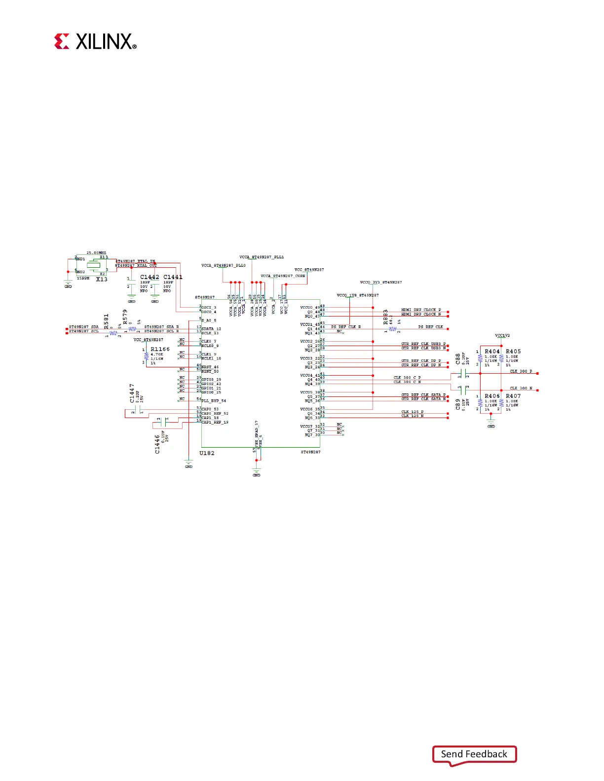
The IDT8T49N287A-501NLGI U182 (located on the bottom of the board) is a one-time
programmable clock source with frequency adjustment available over the I2C bus. The clock
circuit is shown in Figure 3-8.
For more details, see the IDT8T49N287A data sheet [Ref 21].
X-Ref Target - Figure 3-8
Figure 3-8: IDT8T49N287 Clock Generator

 Loading...


