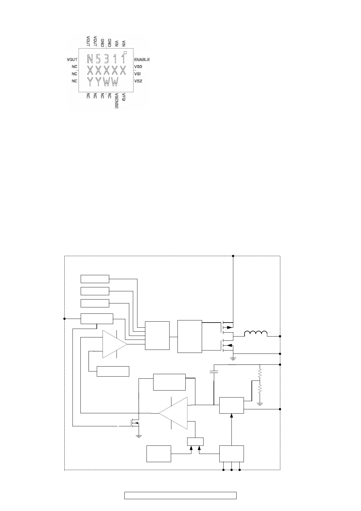
V
IN
(Pin 1,2): Input voltage pin. Supplies power
to the IC. VIN can range from 2.4V to 5.5V.
Input GND: (Pin 3): Input power ground.
Connect this pin to the ground terminal of the
input capacitor. Refer to Layout
Recommendations for further details.
Output GND: (Pin 4): Power ground. The
output filter capacitor should be connected
between this pin and V
OUT
. Refer to Layout
recommendations for further detail.
V
OUT
(Pin 5,6,7): Regulated output voltage.
NC (Pin 8,9,10,11,12,13,14): These pins
should not be electrically connected to each
other or to any external signal, voltage, or
ground. One or more of these pins may be
connected internally.
V
SENSE
(Pin 15): Sense pin for output voltage
regulation. Connect V
SENSE
to the output
voltage rail as close to the terminal of the
output filter capacitor as possible.
V
FB
(Pin 16): Feed back pin for external divider
option. When using the external divider option
(VS0=VS1=VS2= high) connect this pin to the
center of the external divider. Set the divider
such that V
FB
= 0.603V.
VS0,VS1,VS2 (Pin 17,18,19): Output voltage
select. VS0=pin19, VS1=pin18, VS2=pin17.
Selects one of seven preset output voltages or
choose external divider by connecting pins to
logic high or low. Logic low is defined as V
LOW
d 0.4V. Logic high is defined as V
HIGH
t 1.4V.
Any level between these two values is
indeterminate.
ENABLE (Pin 20): Output enable. Enable =
logic high, disable = logic low. Logic low is
defined as V
LOW
d 0.2V. Logic high is defined
as V
HIGH
t 1.4V. Any level between these two
values is indeterminate.
Bottom Thermal Pad: Device thermal pad to
remove heat from package. Connect to PCB
surface ground pad and PCB internal ground
plane (see layout recommendations).
Figure 2. Pin description, top view.
 Loading...