4 - 6
X3
(HPF)
LO
AMP
LPF
PLL
IC
LPF
LPF
X2
FIL
LOOP
BUFF
BUFF
VCO
SW
VCO
SW
FIL
LOOP
ATT
LPFATT
ATT
BUFF
ATT
-> RX LO signals for 300 MHz band (230-420 MHz) ->
-> RX LO signals for 800MHz band (810-999 MHz) ->
-> RX LO signals for 440 MHz band (420-550 MHz) ->
-> RX LO signals for 140 MHz band (118-174 MHz) ->
140 MHz band
1st IF MIXER
440 MHz band
1st IF MIXER
800 MHz and
300 MHz bands
1st IF MIXER
Q110,111
D145-148
Q73
D87,91,92
Q52
Q76
Q61,62
IC14
IC15
IF IC
TCXO
15.3MHz
PLLSTB
PLLDATA
PLLCK
X5
45.9 MHz
RF
SW
Q79
IC45
D155
LO SW
D102
D101
LO SW
LO SW
D103
LO SW
LO SW
D170
D104
Q124
To VHF TX Aamplifier
To UHF TX Aamplifier
LO SW
D179
LO SW
D181
D180
Q125
Q113
D160,D175
Q 1015
LO SW
VHF VCO
UHF VCO
IC64
SELECT
VCO
IC1018
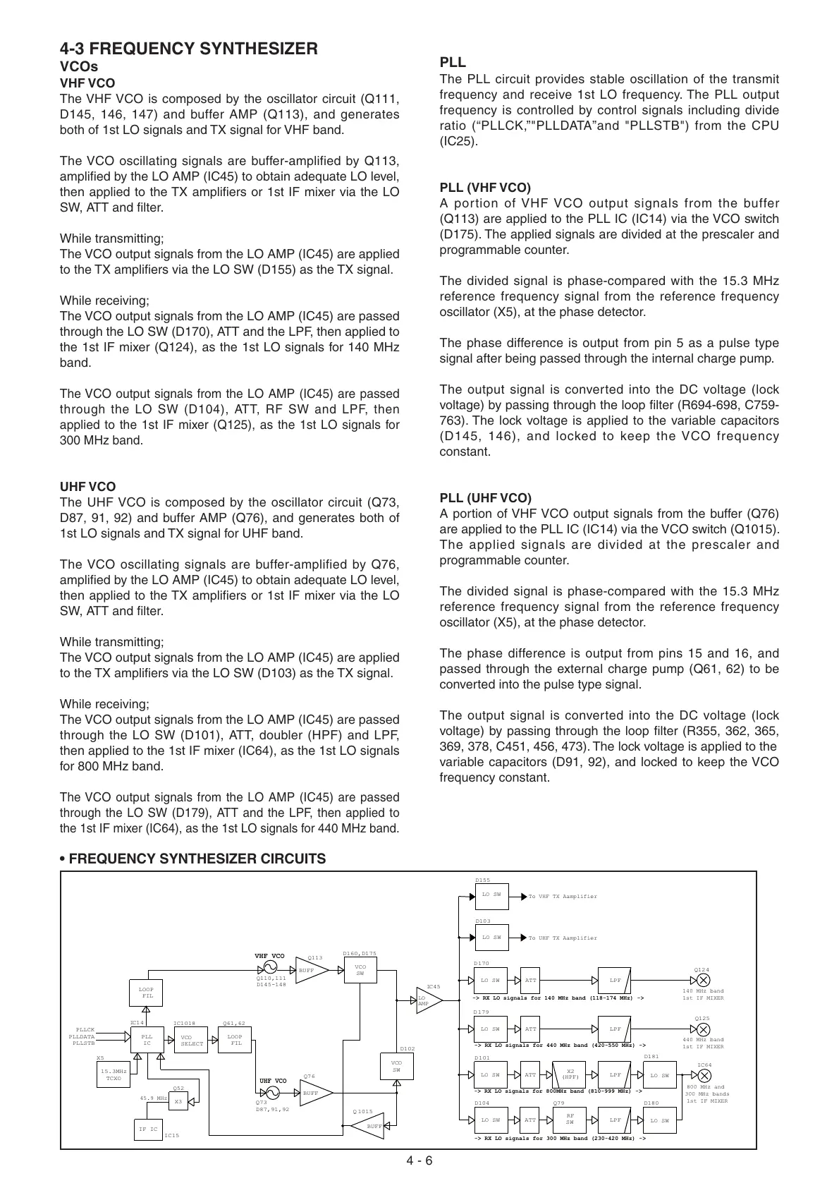
4-3 FREQUENCY SYNTHESIZER
VCOs
VHF VCO
The VHF VCO is composed by the oscillator circuit (Q111,
D145, 146, 147) and buffer AMP (Q113), and generates
both of 1st LO signals and TX signal for VHF band.
The VCO oscillating signals are buffer-amplified by Q113,
amplifi ed by the LO AMP (IC45) to obtain adequate LO level,
then applied to the TX amplifi ers or 1st IF mixer via the LO
SW, ATT and fi lter.
While transmitting;
The VCO output signals from the LO AMP (IC45) are applied
to the TX amplifi ers via the LO SW (D155) as the TX signal.
While receiving;
The VCO output signals from the LO AMP (IC45) are passed
through the LO SW (D170), ATT and the LPF, then applied to
the 1st IF mixer (Q124), as the 1st LO signals for 140 MHz
band.
The VCO output signals from the LO AMP (IC45) are passed
through the LO SW (D104), ATT, RF SW and LPF, then
applied to the 1st IF mixer (Q125), as the 1st LO signals for
300 MHz band.
UHF VCO
The UHF VCO is composed by the oscillator circuit (Q73,
D87, 91, 92) and buffer AMP (Q76), and generates both of
1st LO signals and TX signal for UHF band.
The VCO oscillating signals are buffer-amplified by Q76,
amplifi ed by the LO AMP (IC45) to obtain adequate LO level,
then applied to the TX amplifi ers or 1st IF mixer via the LO
SW, ATT and fi lter.
While transmitting;
The VCO output signals from the LO AMP (IC45) are applied
to the TX amplifi ers via the LO SW (D103) as the TX signal.
While receiving;
The VCO output signals from the LO AMP (IC45) are passed
through the LO SW (D101), ATT, doubler (HPF) and LPF,
then applied to the 1st IF mixer (IC64), as the 1st LO signals
for 800 MHz band.
The VCO output signals from the LO AMP (IC45) are passed
through the LO SW (D179), ATT and the LPF, then applied to
the 1st IF mixer (IC64), as the 1st LO signals for 440 MHz band.
PLL
The PLL circuit provides stable oscillation of the transmit
frequency and receive 1st LO frequency. The PLL output
frequency is controlled by control signals including divide
ratio (“PLLCK,”"PLLDATA”and "PLLSTB") from the CPU
(IC25).
PLL (VHF VCO)
A portion of VHF VCO output signals from the buffer
(Q113) are applied to the PLL IC (IC14) via the VCO switch
(D175). The applied signals are divided at the prescaler and
programmable counter.
The divided signal is phase-compared with the 15.3 MHz
reference frequency signal from the reference frequency
oscillator (X5), at the phase detector.
The phase difference is output from pin 5 as a pulse type
signal after being passed through the internal charge pump.
The output signal is converted into the DC voltage (lock
voltage) by passing through the loop fi lter (R694-698, C759-
763). The lock voltage is applied to the variable capacitors
(D145, 146), and locked to keep the VCO frequency
constant.
PLL (UHF VCO)
A portion of VHF VCO output signals from the buffer (Q76)
are applied to the PLL IC (IC14) via the VCO switch (Q1015).
The applied signals are divided at the prescaler and
programmable counter.
The divided signal is phase-compared with the 15.3 MHz
reference frequency signal from the reference frequency
oscillator (X5), at the phase detector.
The phase difference is output from pins 15 and 16, and
passed through the external charge pump (Q61, 62) to be
converted into the pulse type signal.
The output signal is converted into the DC voltage (lock
voltage) by passing through the loop fi lter (R355, 362, 365,
369, 378, C451, 456, 473). The lock voltage is applied to the
variable capacitors (D91, 92), and locked to keep the VCO
frequency constant.
• FREQUENCY SYNTHESIZER CIRCUITS
 Loading...