4 - 7
4-4 CPU (MAIN UNIT; IC25) PORT ALLOCATION
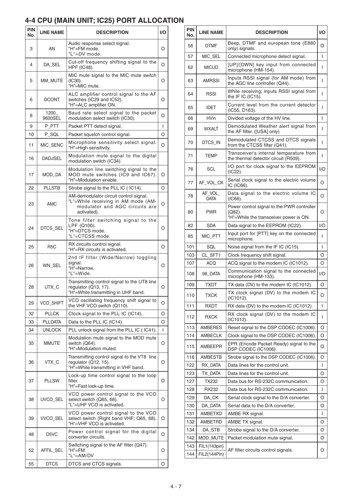
PIN
No.
LINE NAME
DESCRIPTION I/O
3
AN
Audio response select signal.
"H"=FM mode.
"L"=DV mode.
O
4
DA_SEL
Cut-off frequency shifting signal to the
HPF (IC48).
O
5
MM_MUTE
MIC mute signal to the MIC mute switch
(IC30).
"H"=MIC mute.
O
6
DCONT
ALC amplifier control signal to the AF
switches (IC29 and IC52).
"H"=ALC amplifi er ON.
O
8
1200_
9600SEL
Baud rate select signal to the packet
modulation select switch (IC30).
O
9
P_PTT
Packet PTT detect signal. I
10
P_SQL
Packet squelch control signal. O
11
MIC_SENC
Microphone sensitivity select signal.
"H"=High sensitivity.
O
16
DADJSEL
Modulation mute signal to the digital
modulation switch (IC34).
17
MOD_DA
Modulation line switching signal to the
MOD mute switches (IC9 and IC67).
"H"=Modulation enable.
O
22
PLLSTB
Strobe signal to the PLL IC ( IC14). O
23
AMC
AM-demodulator circuit control signal.
"L"= While receiving in AM mode (AM-
modulator and AGC circuits are
activated).
O
24
DTCS_SEL
Tone filter switching signal to the
LPF (Q100).
"H"=DTCS mode.
"L"=CTCSS mode.
O
25
R5C
RX circuits control signal.
"H"=RX circuits is activated.
O
26
WN_SEL
2nd IF filter (Wide/Narrow) toggling
signal.
"H"=Narrow.
"L"=Wide.
O
28
UTX_C
Transmitting control signal to the UT8 line
regulator (Q13, 17).
"H"=While transmitting in UHF band.
O
29
VCO_SHIFT
VCO oscillating frequency shift signal to
the VHF VCO switch (Q110).
O
32
PLLCK
Clock signal to the PLL IC (IC14). O
33
PLLDATA
Data to the PLL IC (IC14). O
34
UNLOCK
PLL unlock signal from the PLL IC ( IC41). I
35
MMUTE
Modulation mute signal to the MOD mute
switch (Q64).
"H"=Modulation muted.
O
36
VTX_C
Transmitting control signal to the VT8 line
regulator (Q12, 15).
"H"=While transmitting in VHF band.
O
37
PLLSW
Lock-up time control signal to the loop
fi lter.
"H"=Fast lock-up time.
O
38
UVCO_SEL
VCO power control signal to the VCO
select switch (Q65, 68).
"L"=UHF VCO is activated.
O
39
VVCO_SEL
VCO power control signal to the VCO
select switch (Right band VHF; Q65, 68).
"H"=VHF VCO is activated.
O
48
D5VC
Power control signal for the digital
converter circuits.
O
52
AFFIL_SEL
Switching signal to the AF fi lter (Q47).
"H"=FM
"L"=AM/DV
O
55
DTCS
DTCS and CTCS signals. O
PIN
No.
LINE NAME
DESCRIPTION I/O
56
DTMF
Beep, DTMF and european tone (E880
only) signals.
O
57
MIC_SEL
Connected microphone detect signal. I
62
MICUD
[UP]/[DWN] key input from connected
microphone (HM-154).
I
63
AMRSSI
Inputs RSSI signal (for AM mode) from
the AGC line controller (Q44).
I
64
RSSI
While receiving; inputs RSSI signal from
the IF IC (IC15).
I
65
IDET
Current level from the current detector
(IC55, D163).
I
66
HVin
Divided voltage of the HV line. I
69
WXALT
Demodulated Weather alert signal from
the AF fi lter. ([USA] only)
I
70
DTCS_IN
Demodulated CTCSS and DTCS signals
from the CTCSS fi lter (Q41).
I
71
TEMP
Transceiver's internal temparature from
the thermal detector circuit (R509).
I
76
SCL
I/O port for clock signal to the EEPROM
(IC22).
I/O
77
AF_VOL_CK
Serial clock signal to the electric volume
IC (IC66).
O
78
AF_VOL_
DATA
Data signal to the electric volume IC
(IC66).
O
80
PWR
Power control signal to the PWR controller
(Q82).
"H"=While the transceiver power is ON.
O
82
SDA
Data signal to the EEPROM (IC22). I/O
85
MIC_PTT
Input port for [PTT] key on the connected
microphone.
I
101
SQL
Noise signal from the IF IC (IC15). I
103
CL_SFT1
Clock frequency shift signal. O
107
ACQ
ACQ signal to the modem IC (IC1012). O
108
98_DATA
Communication signal to the connected
microphone (HM-133).
I/O
109
TXDT
TX data (DV) to the modem IC (IC1012). O
110
TXCK
TX clock signal (DV) to the modem IC
(IC1012).
O
111
RXDT
RX data (DV) to the modem IC (IC1012). I
112
RXCK
RX clock signal (DV) to the modem IC
(IC1012).
I
113
AMBERES
Reset signal to the DSP CODEC (IC1006). O
114
AMBECLK
Clock signal to the DSP CODEC (IC1006). O
115
AMBEEPR
EPR (Encode Packet Ready) signal to the
DSP CODEC (IC1006).
O
116
AMBESTB
Strobe signal to the DSP CODEC (IC1006).
O
122
RX_DATA
Data lines for the control unit. I
123
TX_DATA
Data lines for the control unit. O
127
TX232
Data bus for RS-232C communication. O
128
RX232
Data bus for RS-232C communication. I
129
DA_CK
Serial clock signal to the D/A converter. O
130
DA_DATA
Serial data to the D/A converter. O
131
AMBETXD
AMBE RX signal. I
132
AMBETRD
AMBE TX signal. O
134
DA_STB
Strobe signal to the D/A converter. O
142
MOD_MUTE
Packet modulation mute signal. O
143
FIL1(143pin)
AF fi lter circuits control signals. O
144
FIL2(144Pin)
 Loading...