Service Information
4-16
NOTE
Observe the soldering and cleaning pre-
cautions discussed in paragraph 4.2.2
when making board modifications. Circuit
board contamination may degrade card
performance.
Table 4-3
Troubleshooting procedure
Step Item/component Required condition Comments
1 Digital ground P1034, pin 1, 3, 5 All voltages referenced to digital
ground.
2 P1034, pin 9 +5VDC Card power supply voltage.
3 U101, pin 2 CLOCK pulses Serial clock pulses.
4 U101, pin 3 DATA pulses Serial data pulses.
5 U101, pin 7 STROBE pulse End of relay update sequence.
6 U101-U103, pins 10-18 Low when relay state is changed. High
when relay is not changing state.
Relay driver outputs.
7 U105, pin 2 +54.63mV @ 0°C, or +59.23mV
@ +23°C
Reference junction output (see para-
graph 4.3.4).
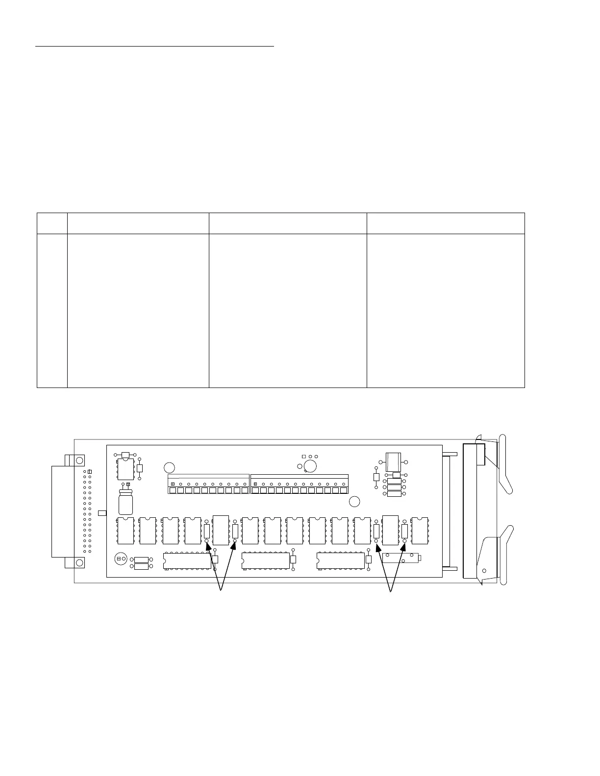
Figure 4-10
Current-limiting resistor locations
HI LO
CH 2 OUT A OUT B
HI LO
CH 3
HI LO
CH 4
HI LO
CH 5
HI LO
CH 6
HI LO
CH 7
HI LO
CH 8
HI LO
CH 9
HI LO
CH 10
HI LO HI LO
Channel 5
Current-limiting
Resistors
Channel 10
Current-limiting
Resistors
unsolder the current-limiting resistors, then solder jumpers
wires in their places. Jumper part number J-3 may be ordered
directly from Keithley Instruments, Inc.
 Loading...