Transmitter (for ATEX specified models) 1-3
3.0 Transmitter (for ATEX specified models)
3.1 General
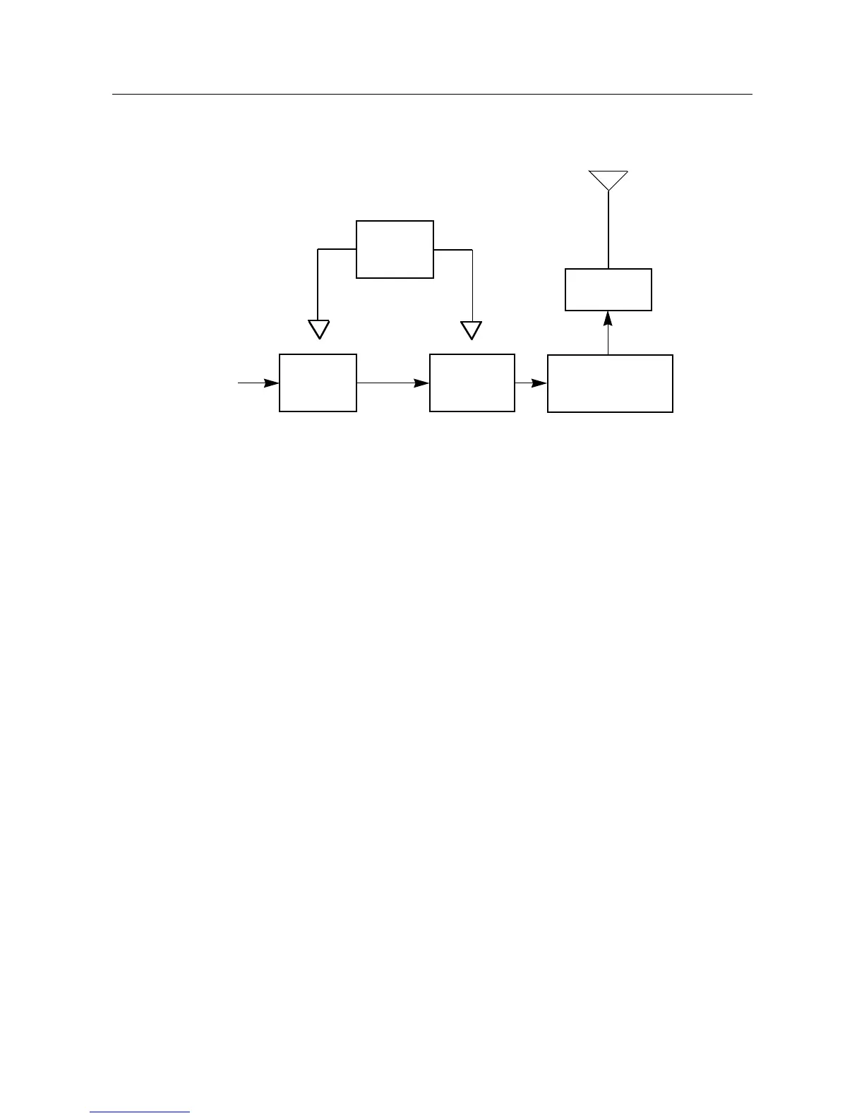
(Refer to Figure 6-1)
The UHF transmitter contains five basic circuits:
1. power amplifier
2. antenna switch
3. harmonic filter
4. antenna matching network
5. power control integrated circuit (PCIC).
3.1.1 Power Amplifier
The power amplifier consists of two devices:
1. 30C65 LDMOS driver IC (U101) and
2. MRF1513 LDMOS PA (Q110).
The 30C65 LDMOS driver IC contains a 2 stage amplification with a supply voltage of 7.3V.
This RF power amplifier is capable of supplying an output power of 0.3W (pin 6 and 7) with an input
signal of 2mW (3dBm) (pin11). The current drain would typically be 160mA while operating in the
frequency range of 403-470MHz.
The MRF1513 LDMOS PA is capable of supplying an output power of 3W with an input signal of
0.3W. The current drain would typically be 650mA while operating in the frequency range of 403-
470MHz. The power output can be varied by changing the biasing voltage.
Controlled voltage of driver IC and PA are limited by dual shunt Zener diodes. This is to limit the RF
power available to the RF connector to less than 2W under fault conditions as per ATEX
requirements.
Figure 1-2: Transmitter Block Diagram
PCIC
Antenna
PA
Antenna Switch/
Driver
Harmonic Filter/
Vcontrol
Vcontrol
From VCO
Jack
PA-Final
Stage
Matching Network
 Loading...