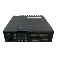
800 MHz Receiver 1-3
3.0 800 MHz Receiver
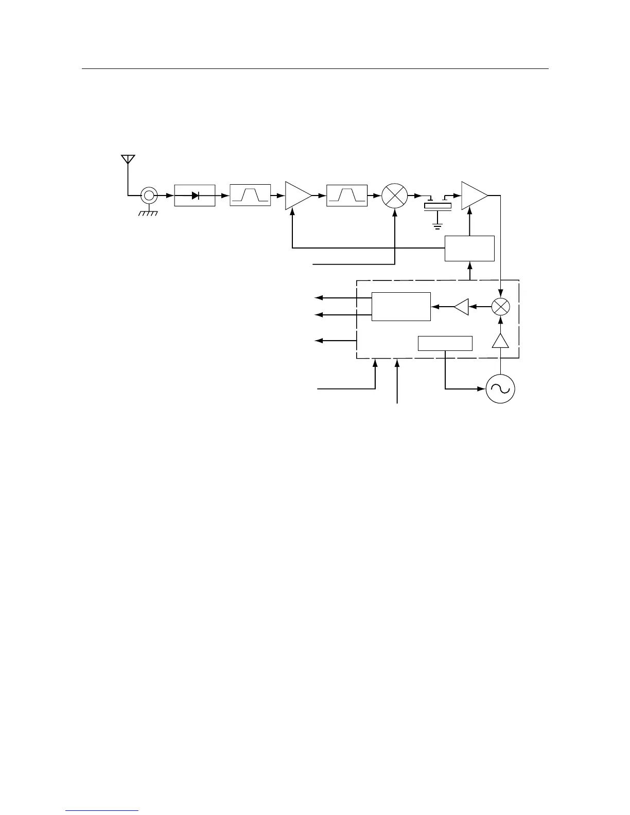
The receiver functions are shown in Figure 2-20 and are described in the paragraphs that follow.
Figure 1-2 800 MHz Receiver Block Diagram.
3.1 Receiver Front-End
(Refer to Figure 2-2 and the UHF Receiver Front End schematic diagram)
The RF signal is received by the antenna and applied to a low-pass filter. For 800 MHz, the filter
consists of L101, L102, C104, C105, C106, C107, C109. The filtered RF signal is passed through the
antenna switch. The antenna switch circuit consists of two PIN diodes(CR101 and CR102) and a pi
network (C109, L103 and C110).The signal is then applied to a fixed tuned ceramic bandpass filter,
FL300.
The output of the bandpass filter is coupled to the RF amplifier transistor Q302 via C300. The RF
amplifier provides a gain of approximately 12 dB. After being amplified by the RF amplifier, the RF
signal is further filtered by a second fixed tuned ceramic bandpass filter, FL301.
Both the pre and post-RF amplifier ceramic filters have similar responses. The insertion loss of each
filter across the 851-870
MHz band is typically 1.8 dB.
The output of the post-RF amplifier filter is connected to the passive double balanced mixer, U301.
After mixing with the first LO signal from the voltage controlled oscillator (VCO) using low side
injection, the RF signal is down-converted to the 109.65
MHz IF signal.
Demodulator
Synthesizer
Crystal
Filter
Mixer
RF
Amp
IF
Amp
3-Pole
Ceramic
Block Filter
3-Pole
Ceramic
Block Filter
Antenna
First LO
from FGU
Recovered Audio
Squelch
RSSI
IF
IC
SPI Bus
16.8 MHz
Reference Clock
Second
LO VCO
RFJack
Pin Diode
Antenna
Switch
AGC
Processing
U351
 Loading...