LTE Standard Module Series
EC200T Series Hardware Design
EC200T_Series_Hardware_Design 61 / 90
4.1.3. Reference Design of RF Antenna Interface
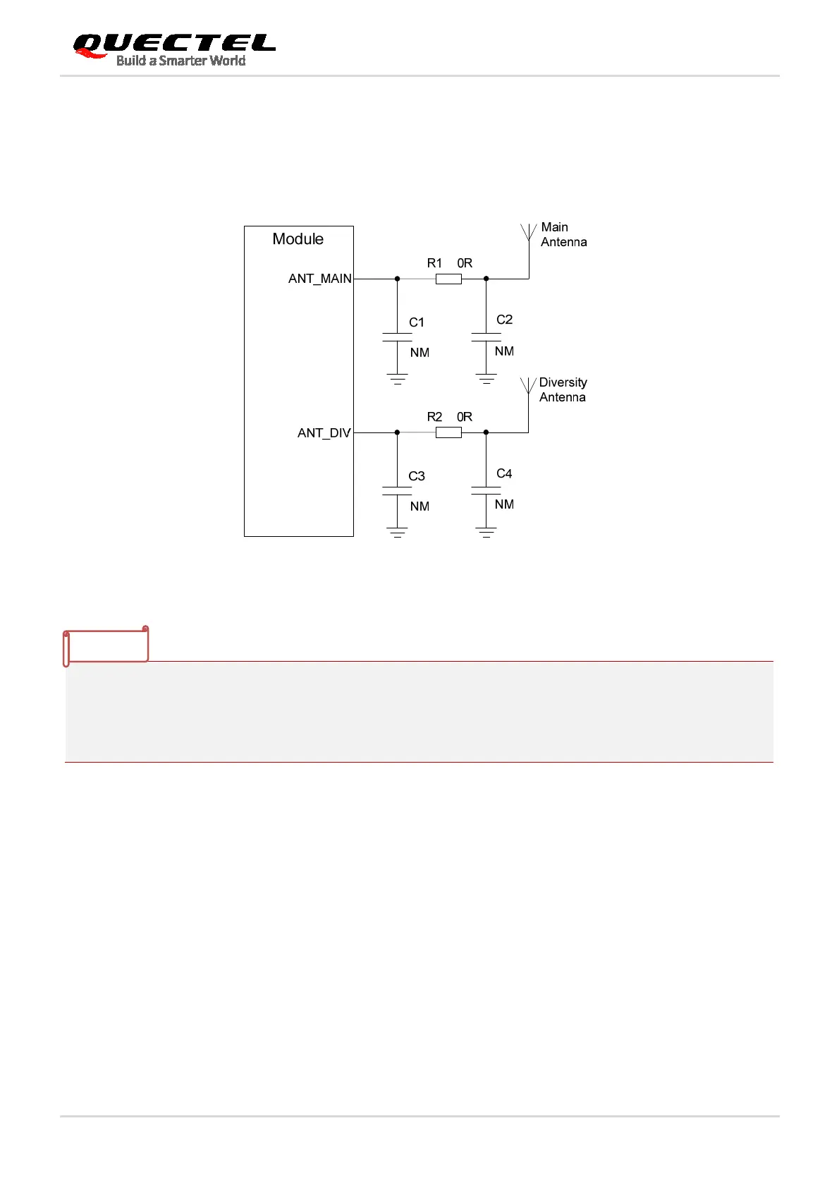
A reference design of ANT_MAIN and ANT_DIV antenna pads is shown as below. A π-type matching
circuit should be reserved for better RF performance. The capacitors are not mounted by default.
Figure 28: Reference Circuit of RF Antenna Interface
1. Keep a proper distance between the main antenna and the Rx-diversity antenna to improve the
receiving sensitivity.
2. Place the π-type matching components (R1 & C1 & C2 and R2 & C3 & C4) as close to the antenna
as possible.
4.1.4. Reference Design of RF Layout
For user’s PCB, the characteristic impedance of all RF traces should be controlled as 50 Ω. The
impedance of the RF traces is usually determined by the trace width (W), the materials’ dielectric constant,
height from the reference ground to the signal layer (H), and the space between the RF trace and the
ground (S). Microstrip and coplanar waveguide are typically used in RF layout to control characteristic
impedance. The following figures are reference designs of microstrip or coplanar waveguide with different
PCB structures.
NOTES
 Loading...