 Loading...
Do you have a question about the Sony STR-DE695 and is the answer not in the manual?
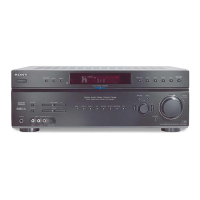
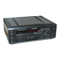
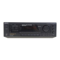
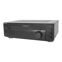
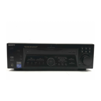
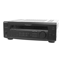
| Dimensions (WxDxH) | 430 x 310 x 157 mm |
|---|---|
| Power requirements | 230 V; 50/60 Hz |
| Supported radio bands | FM, MW |
| Radio Data System (RDS) | Yes |
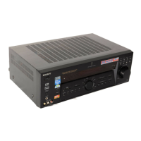
| I/O ports | 5.1 Analogue Input - 1.0 Audio Input - 3.0 Audio Input Front - 1 Audio Output - 1.0 Control A1 / A1 II Digital Input: coaxial - 1.0 Digital Input: optical - 3.0 Digital Output: optical - 1.0 Headphone Output Monitor Output (Picture): FBAS - 1.0 Monitor Output (Picture): S-Video - 1.0 Speaker Selector A, B, A+B S-Video Input - 3.0 S-Video Output- 1.0 Video Input - 4.0 Video Output - 1.0 |
| Connectivity technology | Wired |
| Power consumption (standby) | 0.3 W |
| Power consumption (typical) | 250 W |
| Weight | 8500 g |
|---|
Details on power output and total harmonic distortion for various load conditions.
Procedure for checking AC leakage current from exposed metal parts to earth ground.
Detailed pin descriptions for ICs used in the digital board.
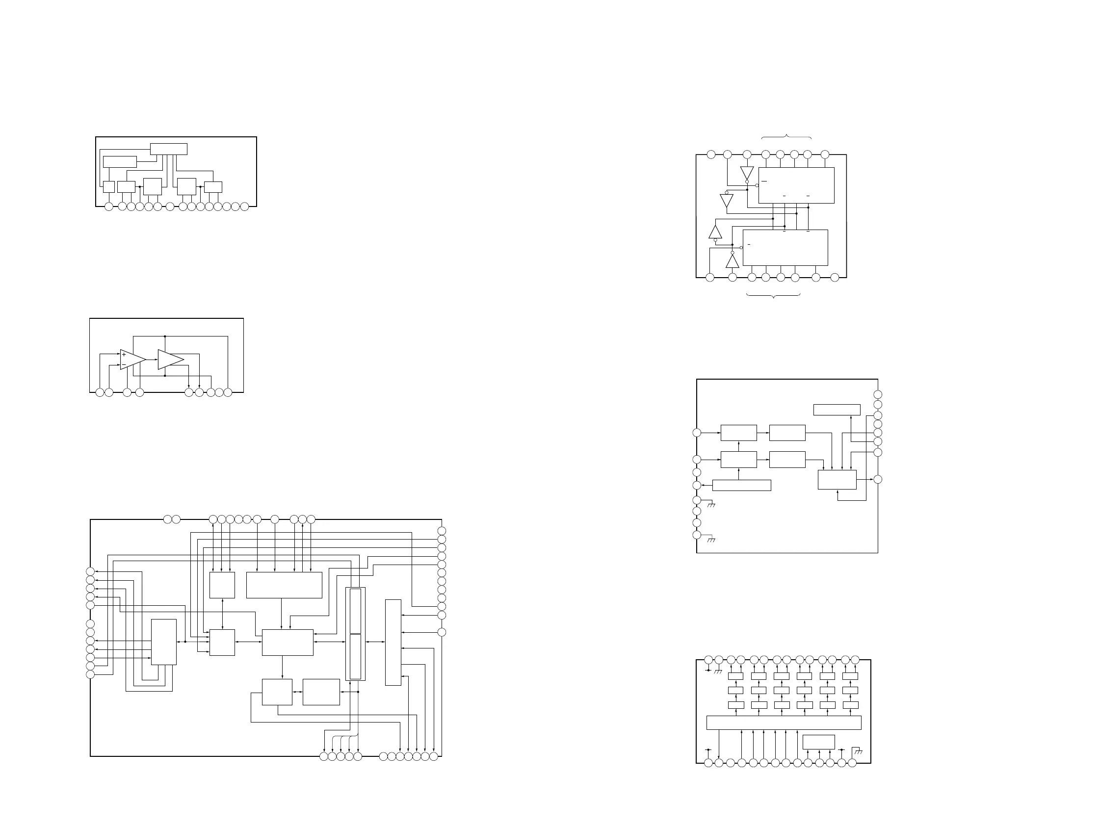
Block diagram illustrating the signal flow of the tuner and audio sections.
Schematic diagram of the main board, part 1 of 3.
Printed wiring board layout for the digital section, part 1 of 2.
Schematic diagram illustrating the video signal processing circuitry.
Schematic diagram detailing the speaker output and protection circuitry.
Printed wiring board layout for the power supply section.
Block diagrams illustrating the internal logic of key ICs.