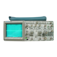
Theory of Operation— 2230 Service
characters are turned on and if any portions of the display
will be intensified more than the rest. Further amplification
of the combined signal sources provides the amplitude lev
els required to drive the crt.
The Z-Axis signal is applied to the crt DC Restorer cir
cuit where it is shifted to the large negative potential used
by the crt. The potential controls the amount of current
supplied by the electron beam to the crt phosphors.
Power Supply
Operating potentials for the instrument are obtained
from a power supply that consists of the Preregulator,
Inverter and Transformer, and Rectifiers and Filters.
Approximately +42 V is supplied by the Preregulator to
drive the 20 kHz Inverter stage through the Transformer
primary windings. The transformer secondary windings
produce the various ac levels that are rectified and filtered
to provide the supply voltages for the instrument’s cir
cuitry. A High Voltage Multiplier circuit produces the
accelerating, focus, and cathode potentials used by the
crt.
Probe Adjust
A front-panel PROBE ADJUST output is provided for
use in adjusting probe compensation. The voltage at the
PROBE ADJUST connector is a negative-going square
wave that has a peak-to-peak amplitude of approximately
0.5 V with a repetition rate of approximately 1 kHz.
Communications Options
Options for this instrument provide a choice of either an
IEEE-488 GPIB (General Purpose Interface Bus) or an
RS-232-G serial output port. The options allow the
transfer of stored waveforms and the control of certain
instrument functions.
DETAILED CIRCUIT DESCRIPTION
The detailed circuit description of the 2230 first
describes the analog operating portion of the oscilloscope
followed by the digital portion. During the description of
the analog circuitry, references are made to circuitry that
either provides information to the Microprocessor or is
controlled by the instrument’s storage circuitry.
ANALOG CIRCUITRY
The instrument has full conventional oscilloscope capa
bilities with all the associated analog circuitry. Signal
pickoff points and signal insertion points connect the ana
log portion of the instrument to the digital operating
system to acquire and display the stored waveforms. The
digital circuitry enhances the analog display by providing
crt readouts of the VOLTS/DIV, SEC/DIV, and Delay Time
Position control settings.
VERTICAL ATTENUATORS
The Channel 1 and Channel 2 Attenuator circuits,
shown on Diagram 1, are identical with the exception of
the additional Invert circuitry in the Channel 2 Paraphase
Amplifier. Therefore, only the Channel 1 Attenuator is
described, with the Invert circuitry of Channel 2 discussed
separately.
The Attenuator circuit and switches (see Figure 3-2)
provide control of the input coupling, the vertical deflection
factor, and the variable volts/division gain. Vertical input
signals for display on the crt or for acquisition by the
storage circuitry may be connected to either or both the
CH 1 OR X and the CH 2 OR Y input connectors. In the
X-Y mode of operation, the signal applied to the CH 1 OR
X connector provides horizontal (X-axis) deflection for the
display, and the signal applied to the CH 2 OR Y connec
tor provides the vertical (Y-axis) deflection for the display.
Switch contacts on the A14 CH 1 Logic board are read
by the Microprocessor to find the CH 1 VOLTS/DIV switch
and Input Coupling switch settings. A switch contact asso
ciated with CH 1 CAL control R43 (Variable Volts/Div) is
also read to see whether that control is in or out of the
calibrated (CAL) detent.
Input Coupling (AC-GND-DC)
A signal from the CH 1 OR X input connector may be
ac or dc coupled to the High-Impedance Attenuator circuit
or disconnected completely by the Input Coupling Switch.
Signals from the CH 1 OR X input connector are routed
through resistor R1 to Input Coupling switch SI. When SI
is set for dc coupling, the Channel 1 signal goes directly to
the input of the High-Impedance Attenuator stage. When
3-7

 Loading...