SP605 Hardware User Guide www.xilinx.com 17
UG526 (v1.9) February 14, 2019
Detailed Description
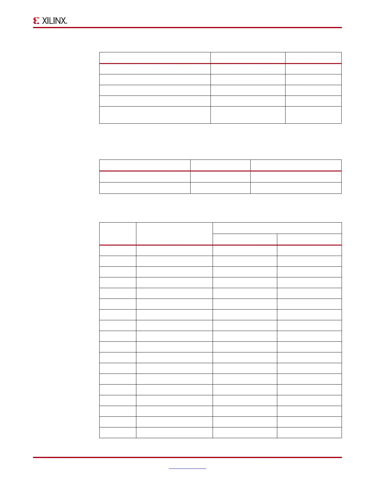
Table 1-5 shows the connections and pin numbers for the DDR3 Component Memory.
MEM1_ODT 4.7 KΩ to GND –
MEM1_DQ[15:0] – ODT
MEM1_UDQS[P,N], MEM1_LDQS[P,N] – ODT
MEM1_UDM, MEM1_LDM – ODT
MEM1_CK[P,N]
100Ω differential at memory
component
–
Notes:
1. Nominal value of V
TT
for DDR3 interface is 0.75V.
Table 1-4: FPGA On-Chip (OCT) Termination External Resistor Requirements
U1 FPGA Pin FPGA Pin Number Board Connection for OCT
ZIO M7 No Connect
RZQ K7 100Ω to GROUND
Table 1-5: DDR3 Component Memory Connections
U1 FPGA
Pin
Schematic Net Name
Memory U42
Pin Number Pin Name
K2 MEM1_A0 N3 A0
K1 MEM1_A1 P7 A1
K5 MEM1_A2 P3 A2
M6 MEM1_A3 N2 A3
H3 MEM1_A4 P8 A4
M3 MEM1_A5 P2 A5
L4 MEM1_A6 R8 A6
K6 MEM1_A7 R2 A7
G3 MEM1_A8 T8 A8
G1 MEM1_A9 R3 A9
J4 MEM1_A10 L7 A10/AP
E1 MEM1_A11 R7 A11
F1 MEM1_A12 N7 A12/BCN
J6 MEM1_A13 T3 NC/A13
H5 MEM1_A14 T7 NC/A14
J3 MEM1_BA0 M2 BA0
J1 MEM1_BA1 N8 BA1
H1 MEM1_BA2 M3 BA2
Table 1-3: Termination Resistor Requirements (Cont’d)
Signal Name Board Termination On-Die Termination

 Loading...


