ZC702 Board User Guide www.xilinx.com 10
UG850 (v1.7) March 27, 2019
Overview
°
Quad SPI flash memory
°
USB JTAG configuration port (Digilent module)
°
Platform cable header JTAG configuration port
°
20-pin PL PJTAG header
°
20-pin PS JTAG header
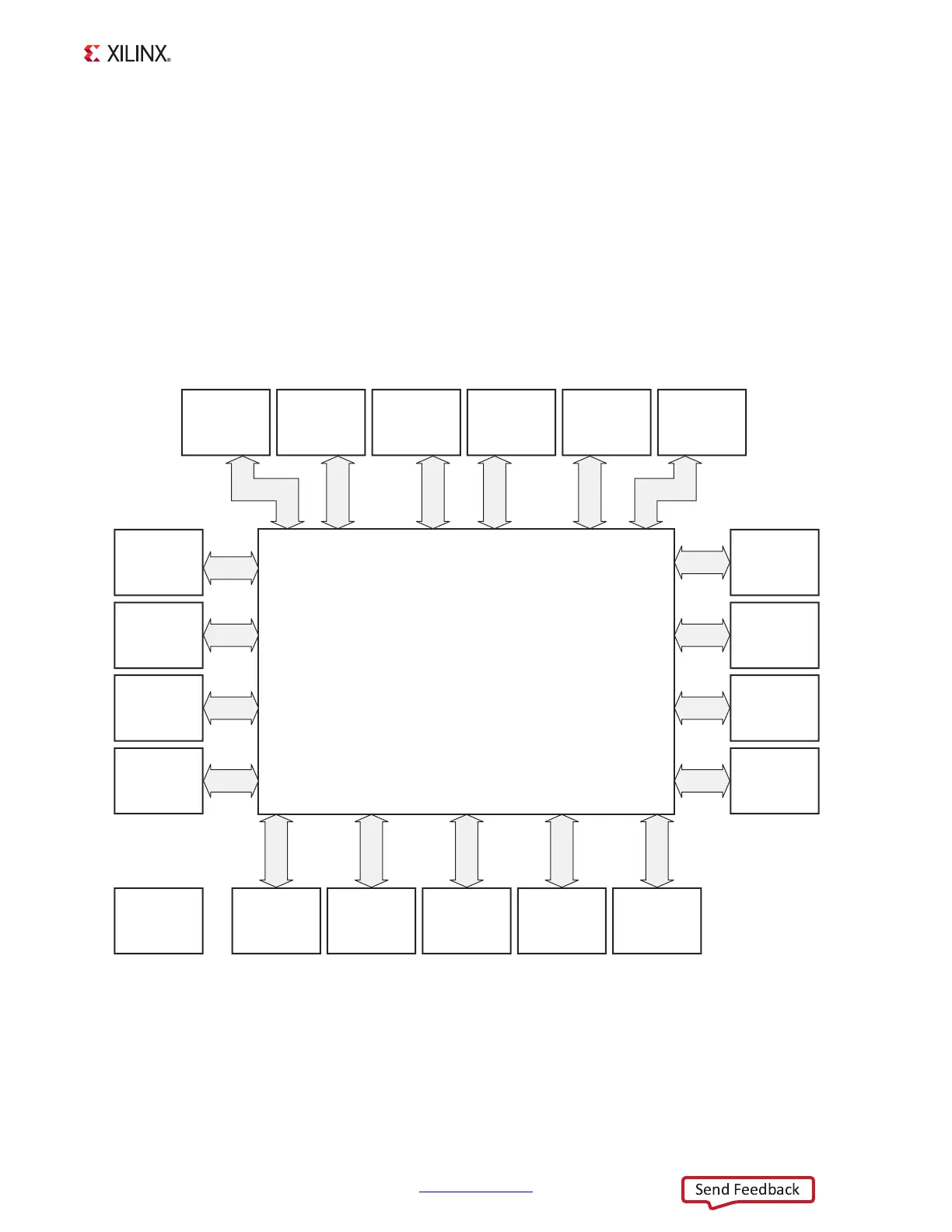
Block Diagram
The ZC702 board block diagram is shown in Figure 1-1.
X-Ref Target - Figure 1-1
Figure 1-1: ZC702 Board Block Diagram
U1
Zynq-7000 SoC
XC7Z020-1CLG484C
Processing
System
Programmable Logic
UG850_c1_01_062918
JTAG Module
and
Connector
Page 15
Quad SPI
Flash Memory
Page 20
CAN Bus
Page 21
SD Card
Connector
Page 22
FMC1 LPC
Connector
Page 23
10/100/1,000
Ethernet PHY
(RGMII only)
Page 26
USB 2.0 ULPI
Transceiver
and Connector
Page 27
JTAG Header
Page 15
USB UART
Page 36
ARM PJTAG
Header
Page 35
Switches
LEDs and
Pushbuttons
Page 34
Mechanicals
Page 38
I
2
C
Real Time
Clock
Page 33
Clock and
Reset/POR
Pushbuttons
Page 14
DDR3 Memory
4 x 256 Mb x 8
SDRAM
Pages 16-19
HDMI Codec
and
Connector
Page 28, 29
I
2
C Multiplexer
and
I
2
C EEPROM
Page 32
XADC
Header
Page 31
Configurable
Clocks
Page 30
FMC2 LPC
Connector
Page 24
Note: Page numbers reference the page number of schematic 0381449.

 Loading...