ZC702 Board User Guide www.xilinx.com 30
UG850 (v1.7) March 27, 2019
Feature Descriptions
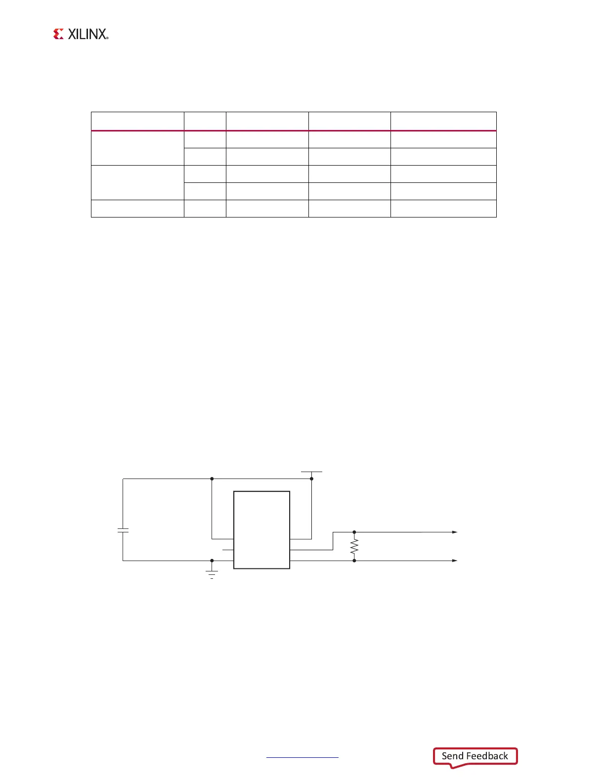
Table 1-12 lists the pin-to-pin connections from each clock source to the XC7Z020 SoC.
System Clock
[Figure 1-2, callout 7]
The system clock source is an LVDS 200 MHz oscillator at U43. It is wired to a multi-region
clock capable (MRCC) input on programmable logic (PL) bank 35. The signal pair is named
SYSCLK_P and SYSCLK_N and each signal is connected to U1 pins D18 and C19 respectively
on the XC7Z020 SoC.
• Oscillator: SiTime SiT9102AI-243N25E200.00000 (200 MHz)
• Frequency Tolerance: 50 ppm
• Differential Output
For more details, see the SiTime SiT9102 data sheet [Ref 18]. The system clock circuit is
shown in Figure 1-11.
Table 1-12: Clock Connections, Source to XC7Z020 SoC
Clock Reference Pin Net Name I/O Standard XC7Z020 (U1) Pin
U43
5SYSCLK_N LVDS_25 C19
4SYSCLK_P LVDS_25 D18
U28
5 USRCLK_N LVDS_25 Y8
4 USRCLK_P LVDS_25 Y9
U65 3 PS_CLK NA F7 (Bank 500)
X-Ref Target - Figure 1-11
Figure 1-11: System Clock Source
UG850_c1_11_030513
GND
VCC2V5
SIT9102
200 MHz
Oscillator
OE
NC
GND
VCC
OUT_B
OUT
1
2
3
6
5
4
U43
R168
100Ω 1%
SYSCLK_P
SYSCLK_N
C71
0.1 μF 10V
X5R

 Loading...