ZC702 Board User Guide www.xilinx.com 40
UG850 (v1.7) March 27, 2019
Feature Descriptions
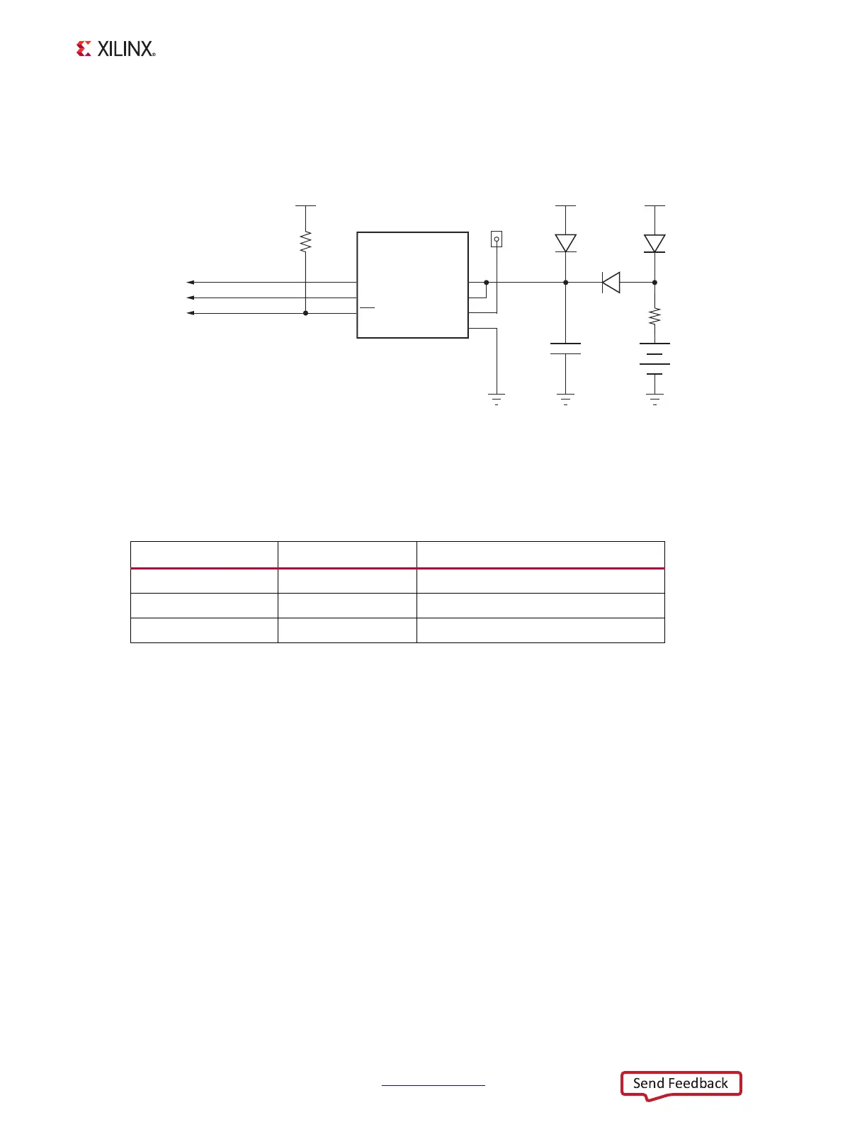
Figure 1-17 shows the real-time clock circuit.
Real-time clock connections to the XC7Z020 SoC and the PCA9548 8-Channel bus switch
are listed in Table 1-20.
Information about the RTC-8564JE is available at the Epson Electronics America website
[Ref 22].
I/O Expansion Header
[Figure 1-2, callout 16]
The 2 x 6 I/O expansion header J54 supports Digilent Pmod Peripheral Modules. 8 pins
(IIC_PMOD[0:7]) are connected to the TI TCA6416APWR I2C expansion port device U80. See
the Digilent website for information on Digilent Pmod Peripheral Modules [Ref 23].
X-Ref Target - Figure 1-17
Figure 1-17: Real Time Clock Circuit
Table 1-20: Real Time Clock Connections
RTC-8564JE (U16) Pin Net Name Connects To
6 IIC_RTC_SCL U44.11 (PCA9548 SC4)
7 IIC_RTC_SDA U44.10 (PCA9548 SD4)
10 IIC_RTC_IRQ_1_B
(1)
U1.U7 (XC7Z020 SoC PL BANK 13)
Notes:
1. I/O standard = LVCMOS_25.
UG850_c1_17_032719
VCC3V3 VCC2V5
VADJ
GND
IIC_RTC_SCL
B2
NBL-621/N9D
2V
C217
0.01μF
25V
X7R
1
J39
YELLOW
IIC_RTC_IRQ_1_B
IIC_RTC_SDA
D6
BAT54T1G
30V 400 mW
RTC-8564JE
Real Time Clock
Module
7
6
10
U16
16
15
14
13
INT
SCL
SDA
GND
CLKOUT
CLKOE
VCC
D5
BAT54T1G
30V 400 mW
D7
BAT54T1G
30V 400 mW
GND
GND
R187
10.0K
0.1Ω
R249
4.7K

 Loading...