Do you have a question about the Yamaha HTR-6030 and is the answer not in the manual?
Warns about personal injury and product damage from improper servicing.
Clarifies that manual provision does not grant service authorization.
Warns of component damage from static discharge.
Advises powering off unit during disassembly and checks.
Emphasizes replacing critical components with exact specifications.
Details leakage current testing for electrical safety.
Warns about lead in solder and potential health risks.
Provides guidance on using lead-free solder for repairs.
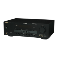
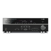
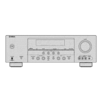
Shows front panel layout for RX-V361 (U, C models).
Shows front panel layout for RX-V361 (R, T, K, A, B, G, E, L models).
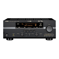
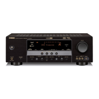
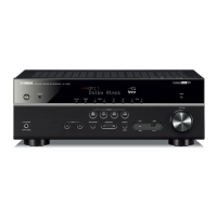
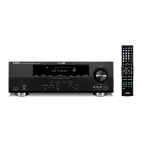
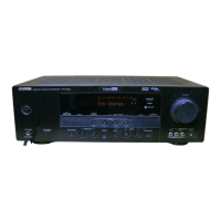
Shows front panel layout for HTR-6030 (U, C models).
Shows front panel layout for HTR-6030 (R, T, K, A, G, E models).
Shows front panel layout for DSP-AX361 (J model).
Shows rear panel layout for RX-V361 (U, C models).
Shows rear panel layout for RX-V361 (R model).
Shows rear panel layout for RX-V361 (T model).
Shows rear panel layout for RX-V361 (K model).
Shows rear panel layout for RX-V361 (A model).
Shows rear panel layout for RX-V361 (B, G, E models).
Shows rear panel layout for RX-V361 (L model).
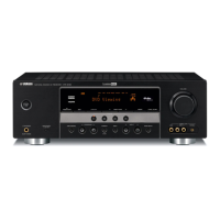
Shows rear panel layout for HTR-6030 (U, C models).
Shows rear panel layout for HTR-6030 (R model).
Shows rear panel layout for HTR-6030 (T model).
Shows rear panel layout for HTR-6030 (K model).
Shows rear panel layout for HTR-6030 (A model).
Shows remote control layout for RAV311.
Shows remote control layout for RAV312.
Shows remote control layout for RAV28.
Details audio output power and related specifications.
Details video signal type and levels.
Lists general specifications like power supply and consumption.
Describes SCENE templates for various listening modes.
Details sound field parameters and surround settings.
Lists supported surround decoding formats.
Provides a table of available settings in the SET MENU.
Identifies major components from the top view.
Identifies major components from the front view.
Step-by-step instructions for removing the top cover.
Instructions for removing the front panel unit.
Steps to remove the MAIN (2) P.C.B.s.
Procedures for removing the DSP P.C.B.
Steps for checking PCBs and ensuring proper grounding.
Lists necessary tools for firmware update.
Step-by-step guide for updating firmware.
How to confirm successful firmware version update.
Lists the available DIAG menu items.
Lists further available DIAG menu items.
Instructions on how to start the DIAG mode.
How to start DIAG with protection function disabled.
Steps to cancel the DIAG mode.
What is displayed when the DIAG mode starts.
Displays when no protection history is found.
Explains protection history due to excess current.
Explains protection history due to abnormal DC output.
Explains protection history due to abnormal power supply voltage.
Explains protection history due to excessive heat sink temperature.
How protection history is stored and cleared.
How to navigate DIAG menus and sub-menus.
Functions available during DIAG mode operation.
Initial settings when starting the DIAG mode.
Details the BYPASS function, analog or DSP output.
Describes the AUDIO CHECK function and output distribution.
Explains SPEAKER SET settings and analog switch configurations.
Details the 6CH INPUT selection and its sub-menus.
Explains the MIC CHECK function for audio output.
Describes the FL display check program.
Explains the TEST TONE function for noise output.
Used for initializing or inhibiting back-up RAM.
Displays A/D conversion values for panel keys and protection functions.
Details A/D conversion values for protection functions.
Details panel key A/D values and checks.
Checks output of XM radio antenna module.
Notes DOCK function applicability.
Notes USB CHECK applicability.
Notes DAB CHECK applicability.
Notes IF STATUS applicability.
Displays A/D setting values for each protection.
Displays past protection histories.
Switches function settings on PCB via software.
Displays firmware version and checksum.
Shows display data for V2001.
Pin assignments for connector V2001.
Anode and grid connections for display segments.
Pin details for ADSP-BF531 CPU.
Continues pin details for ADSP-BF531 CPU.
Continues pin details for ADSP-BF531 CPU.
Pin details for IC204-IC206.
Pin details for IC204.
Pin details for IC205.
Pin details for IC206.
Details IC401 ADC select port.
Pin details for IC401.
Pin details for IC402, IC403.
Pin details for IC402.
Pin details for IC403.
Pin details for IC301 AK4588VQ.
Continues pin details for IC301 AK4588VQ.
Continues pin details for IC301 AK4588VQ.
Pin details for IC161 R2A15215FP.
Continues pin details for IC161 R2A15215FP.
Continues pin details for IC161 R2A15215FP.
Pin details for IC201 M66003-0131FP-R.
Continues pin details for IC201 M66003-0131FP-R.
Block diagram for video, audio, and power supply sections.
Block diagram of the control section.
Pin connection diagrams for various ICs.
Pin connection diagrams for diodes and transistors.
Component layout for DSP P.C.B. (Side A).
Component layout for DSP P.C.B. (Side B).
Component layout for OPERATION (1) P.C.B. (Side A).
Component layout for OPERATION (1) P.C.B. (Side B).
Component layout for OPERATION (2) P.C.B. (Side A).
Component layout for OPERATION (2) P.C.B. (Side B).
Component layout for OPERATION (3) P.C.B. (Side A).
Component layout for OPERATION (3) P.C.B. (Side B).
Component layout for OPERATION (5) P.C.B. (Side A).
Component layout for OPERATION (6) P.C.B. (Side A).
Component layout for OPERATION (6) P.C.B. (Side B).
Component layout for OPERATION (7) P.C.B. (Side A).
Component layout for OPERATION (7) P.C.B. (Side B).
Component layout for OPERATION (10) P.C.B. (Side A).
Component layout for OPERATION (11) P.C.B. (Side A).
Component layout for MAIN (1) P.C.B. (Side A).
Component layout for MAIN (1) P.C.B. (Side B).
Component layout for MAIN (2) P.C.B. (Side A).
Component layout for MAIN (2) P.C.B. (Side B).
Component layout for MAIN (3) P.C.B. (Side A).
Component layout for MAIN (4) P.C.B. (Side A).
Component layout for D-VIDEO P.C.B. (Side A).
Component layout for D-VIDEO P.C.B. (Side B).
Schematic diagram for DSP section (1 of 5).
Schematic diagram for DSP section (2 of 5).
Schematic diagram for DSP section (3 of 5).
Schematic diagram for DSP section (4 of 5).
Schematic diagram for DSP section (5 of 5).
Schematic diagram for Operation 1/2.
Schematic diagram for Operation 2/2.
Schematic diagram for Main 1/2.
Schematic diagram for Main 2/2.
Schematic diagram for D-VIDEO (J model).
Lists electrical components for replacement.
Parts list for the DSP P.C.B.
Continues parts list for the DSP P.C.B.
Parts list for DSP and OPERATION P.C.B.s.
Parts list for OPERATION P.C.B.
Parts list for OPERATION and MAIN P.C.B.s.
Parts list for MAIN P.C.B.
Continues parts list for MAIN P.C.B.
Continues parts list for MAIN P.C.B.
Parts list for MAIN and D-VIDEO P.C.B.s.
Parts list for D-VIDEO P.C.B. and carbon resistors.
Exploded view of the overall assembly with part references.
Lists included accessories like remote controls and cables.
Exploded view of the front panel unit with part references.
Exploded view of the AMP unit with part references.
Schematic diagram of the remote control.
Layouts of different remote control models.
Key number layout for remote controls.
Lists key codes for remote control commands.
Schematic diagram for RAV28 remote control.
Key number layout for RAV28 remote.
Key codes for RAV28 remote control commands.
Sets speaker impedance for optimal performance.
Resets all unit parameters to factory default settings.
Sets tuner frequency step based on region.