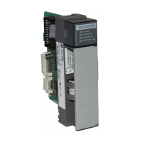
1 Publication 1746-UM004A-US-P
Chapter
4
Programming Overview
This chapter provides an overview of the information needed to program your
module. After reading this chapter, you should be familiar with:
• Module memory organization
• SLC memory allocation for your module
• BASIC programming instructions
• entering, running, and editing a BASIC program from an ASCII terminal
• interfacing the module with other devices
Understanding Module
Memory Organization
All data transferred to the module from the SLC 500 CPU must be routed through
the module input buffer. Table 4.1 lists the addresses of the module input buffer.
All data transferred from the module to the SLC 500 CPU must be routed through
the module output buffer. Table 4.2 lists the addresses of the module output buffer.
Table 4.1 Input Buffer Addresses
Address Definition
0 through 39 Data transferred from the DH485 common interface file.
40 through 99 Reserved
100 through 163 Data transferred from the CPU M0 file.
164 through 199 Reserved
200 through 207 Data transferred from the CPU output image table.
Table 4.2 Output Buffer Addresses
Address Definition
0 through 39 Data transferred to the DH485 common interface file.
40 through 99 Reserved
100 through 163 Data transferred to the CPU M1 file.
164 through 199 Reserved
200 through 207 Data transferred to the CPU input image table.
Spare Allen-Bradley Parts