2
Contents
Safety Information .............................................................................................................................3
Warranty .............................................................................................................................................3
Specifications ................................................................................................................................ 4-5
Electrostatic Discharge Sensitive (ESDS) Device Handling .........................................................5
Part List Notes ...................................................................................................................................5
Product Description ...................................................................................................................... 6-9
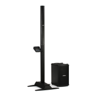
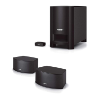
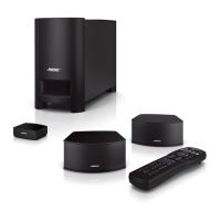
System Components.........................................................................................................................6
Setting up the L1
®
model II power stand .........................................................................................7
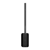
Assembling the L1 model II Cylindrical Radiator
®
loudspeaker ...................................................7
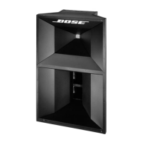
Connecting the B1 bass module .....................................................................................................8
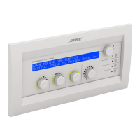
L1 Model II Power Stand Input and Output Connectors, Controls ...............................................8
Setting the Analog Input Level on the L1 Model II Power Stand...................................................9
Adding a T1 ToneMatch
®
audio engine ...........................................................................................9
Packaging Part List, L1 Model II Power Stand (see Figure 1) .....................................................10
Figure 1. L1 Model II Power Stand Packaging View .........................................................................10
Packaging Part List, L1 Model II Line Array (see Figure 2) ......................................................... 11
Figure 2. L1 Model II Line Array Packaging View ............................................................................. 11
Packaging Part List, B1 Bass Module (see Figure 3) ...................................................................12
Figure 3. B1 Bass Module Packaging View ......................................................................................12
Main Part List, Power Stand to Leg Assembly (see Figure 4) .....................................................13
Figure 4. Power Stand to Leg Assembly Exploded View...................................................................13
Main Part List, L1 Model II Power Stand Upper Housing (see Figure 5) ....................................14
Figure 5. Power Stand Upper Housing Exploded View .....................................................................15
Main Part List, L1 Model II Power Stand Cavity and Leg Assembly (see Figure 6) ...................16
Figure 6. Power Stand Cavity and Leg Assembly Exploded View....................................................17
Main Part List, L1 Model II Line Array (see Figure 7) ...................................................................18
Figure 7. L1 Model II Line Array Exploded View ...............................................................................19
Main Part List, L1 Model II Line Array End Cap Assemblies (see Figure 8) ...............................20
Figure 8. L1 Model II Line Array End Cap Assemblies Exploded View .............................................21
Main Part List, B1 Bass Module Exploded View (see Figure 9) ..................................................22
Figure 9. B1 Bass Module Exploded View ........................................................................................22
Electrical Part Lists ................................................................................................................... 23-40
Input/Output PCB Assembly .................................................................................................... 23-33
Power Amplifier PCB Assembly .............................................................................................. 34-40
AC Primary PCB Assembly ............................................................................................................40
Disassembly Procedures ......................................................................................................... 41-46
Test Procedures ........................................................................................................................ 47-50
Appendix .................................................................................................................................... 51-55
Figure 10. L1 Model II Power Stand Wiring Diagram ........................................................................55
Theory of Operation .................................................................................................................. 56-62
Circuit Board Layout Diagrams ............................................................................................... 62-68
Figure 11. AC Input PCB Topside Etch and Layout......................................................................62
Figure 12. AC Input PCB Bottom Etch and Layout ......................................................................62
Figure 13. DSP PCB Topside Etch and Layout .............................................................................63
Figure 14. DSP PCB Bottom Silk and Internal Layer 1 ................................................................64
Figure 15. DSP PCB Bottom Silk and Internal Layer 2 ................................................................65
Figure 16. DSP PCB Bottom Silk and Etch ...................................................................................66
Figure 17. Amplifier/SMPS PCB Topside Etch Layout .................................................................67
Figure 18. Amplifier/SMPS PCB Internal Etch Layer 1 Layout ....................................................67
Figure 19. Amplifier/SMPS PCB Internal Etch Layer 2 Layout ....................................................68
Figure 20. Amplifier/SMPS PCB Bottom Etch Layout .................................................................. 68
Service Manual Revision History ...................................................................................................69
 Loading...