Motorola Confidential Proprietary
V975/V980Theory of Operation
3-8
Draft 1.0
RF WCDMA Receiver
MC13820 (U001)
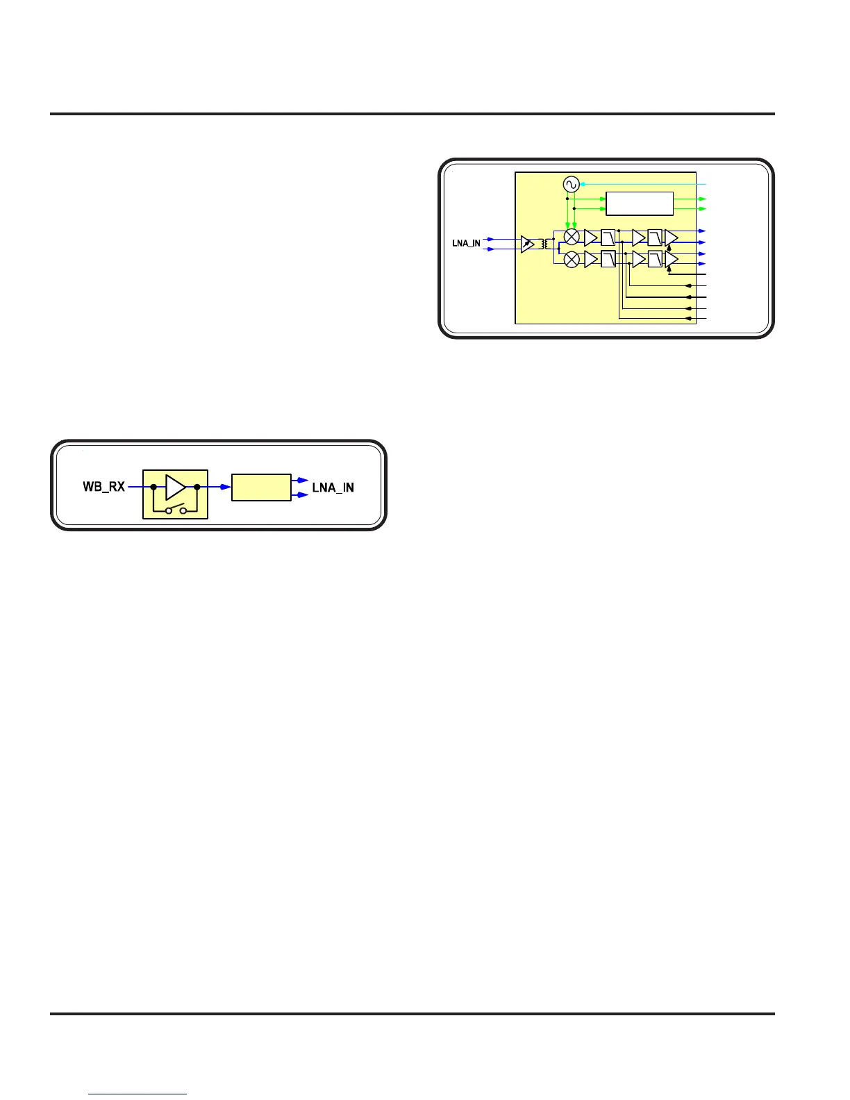
The first IC in the WCDMA Rx line up is U001
(MC13820), which is a Low Noise Amplifier. The RX
frequency will be amplified and passed on to OneLife
WB through FL005. The LNA is controlled by Har-
mony (U100) through two enable lines. MBC_EN1
enables gain for the LNA while MBC_EN2 enables
the IC. Both lines can be probed at testpoints located
near Harmony (TP120 and TP121).
BLUE MODULE (ONELife)
ONELife is a full custom mixed signal BiCMOS IC
with the SiGe option with electroplated copper induc-
tors. This IC is a fully differential direct-conversion front-
end IC and is comprised of a multiband RF section and
a single path baseband section. The RF section is
comprised of three Low Noise Amplifiers, two sets of
quadrature mixers and an integrated 4GHz VCO with
a divided prescaler output. Only one LNA is used in
this design to cover the WCDMA/UMTS band (2110-
1710). The LNA has two gain states; a high gain state
and a bypass state with no reverse isolation. The LNA
drives the quadrature mixers, via an integrated trans-
former matching network, that convert the RF signal to
baseband, quadrature I and Q. The LO signal is pro-
vided by fully integrated VCOs that drives a divide-by-
two quadrature generator. In addition, a divide-by-three/
five circuit is used to feed back the LO signal to the
synthesizer via an open collector output stage.
The baseband section is comprised of two separate I
and Q paths each containing a PMA, an anti-aliasing
filter made up of an IFA with an active pole and DCOC,
two bi-quad sections, and an output buffer. The
baseband signal path has six poles of baseband filtering
distributed between mixer pole, the active IFA pole,
and the two bi-quad blocks. The PMA has pseudo-
continuous gain capability and is part of the AGC sys-
tem along with the LNAs. The PMA AGC is controlled
through five dedicated IC pins. At the output of the PMA
stage, a baseband detector circuit provides broadband,
strong signal information to the baseband part. DC Off-
set correction is provided through external differential
pins to provide offset corrections to the internal IFA
stage. The output buffer receives an input voltage via
feedback from the Harmony WB_CMODE line so that
OneLifeWB’s output signal drives the A/D with the cor-
rect common mode voltage.
Control and programming are done through a SPI in-
terface from Harmony. Two supplies are required to
power the IC, VRF_DIG_1.875V for SPI lines and
VRF_2.775V for RF portions.
Figure 3-10. WCDMA LNA
PMA
BB_OUTIFF AAFIFA
MIXER
RX SYN TH FDBK
/3 OR /5
ONE LIFE
WB_RX_I
WB_RX_IX
WB_RX_Q
WB_RX_QX
WB_DCOC_I
WB_DCOC_IX
WB_DCOC_Q
WB_DCOC_QX
SYNTH_FDBK
WB_RX_TUNE
WB_CMODE
Figure 3-11. ONELife
RF WCDMA Receiver
 Loading...