Motorola Confidential Proprietary
Theory of OperationService Manual(Level 3)
3-9
Draft 1.0
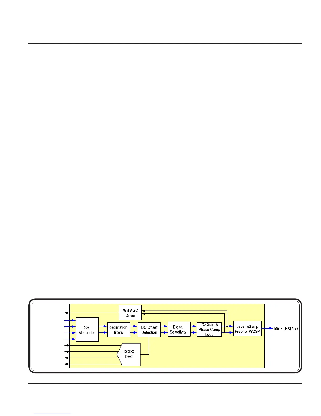
Harmony WCDMA_RX (U100)
The RX I an Q baseband signals are fed into the Sigma-
Delta modulator of the Harmony. The Sigma-Delta
modulator is an A/D converter that converts the I and
Q baseband inputs to noise shaped 6-bit digital out-
puts. These outputs are then next decimated by a ratio
of 3 using 3-stage cascaded comb type filters to a sam-
pling rate of 15.36 MHz.
DC offset correction is performed next immediately to
minimize the amount of delay in this mixed mode con-
trol loop to achieve rapid DC acquisition during nor-
mal mode warmup sequences. The DC offset correc-
tion unit has feedback to the OneLife-WB IC to be
able to correct for DC offsets at the inputs to IF ampli-
fier stage.
The matched selectivity filter is designed such that it
provides the desired selectivity to meet adjacent chan-
nel and blocker specifications in the 2100 and 1800
MHz frequency bands.
I/Q gain and phase imbalance equalization units located
next in the lineup is used to correct for I/Q mismatches
due to both the base station transmitter as well as the
mobile device.
Next, the outputs of the I/Q gain equalization unit feed
into the RF/IF AGC as well as the digital gain compen-
sation control units. These outputs from the I/Q gain
equalizer are used by the AGC unit for on-channel power
detection. In addition, the AGC unit also receives off-
channel power indication from a 2-bit SOS detector
data bus from OneLife-WB IC. The on-channel and
off-channel power levels are used by the RF/IF AGC
unit to control internal and external LNA step attenua-
tor stages as well as the variable gain PMA stage in
OneLife-WB IC.
Two bit control lines are used to control each of the
external LNA step attenuator stages. Alternately, a 1-
bit control line is employed to control the internal LNA
in the OneLife IC. In addition, a 5-bit parallel digital
bus is employed to control the PMA variable gain con-
trol stage in OneLife-WB IC. The AGC unit also sup-
plies the detected RSSI level to the external host de-
vice (e.g. POG IC) based upon the current RF, IF, and
digital baseband gain control settings as well as the on-
channel RSSI detected.
Following the I/Q gain equalization stage, a digital gain
compensation unit is located next. The purpose of this
gain compensation unit is to provide a 6-bit gain com-
pensated output signal to the WCSP unit given that the
input signal’s dynamic range is 13 bits. The 15.36 MHz
rate I and Q outputs are then interleaved in the BBIF
(baseband interface) unit to generate the output I/Q data
at a 30.72 MHz rate on a single 6-bit data bus to the
external host device.
MB_RX_I
MB_RX_IX
MB_RX_Q
MB_RX_QX
HARMONY
(U100)
WB_DCOC_I
WB_D CO C_ IX
WB_DCOC_Q
WB_DCOC_QX
W B_AGC(4:0)
Figure 3-12. Harmony WCDMA RX (U100)
RF WCDMA Receiver
 Loading...