Motorola Confidential Proprietary
Theory of OperationService Manual(Level 3)
3-17
Draft 1.0
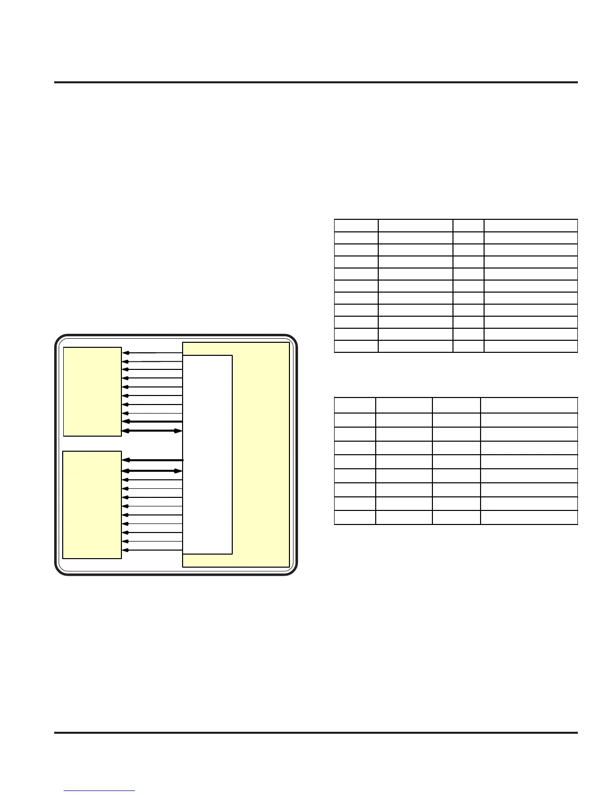
POG Memory
The POG flash memory uses a 128 (128 Mbit) 1.8
Volt wireless memory which delivers high density flash
memory in a single package. Individually erasable
memory blocks are optimally sized for code and data
storage. Four 16-Kword blocks and seven 64-Kword
blocks are located in the parameter partition. The rest
of the flash memory is divided into fifteen partitions of
eight 64-Kword main blocks. By dividing the flash
memory into partitions, program or erase can take place
simultaneously during read operations. The device is
available in a 56-ball vfBGA* package with 0.75 mm
ball pitch.
The POG SDRAM device is a JEDEC standard
SDRAM with 1.8V core supply, 1.8V I/O supply, four
banks, and density of 4Mb x 16 (64 Mb). It is low
power with special function support including partial
array self refresh and temperature compensated refresh.
It has a max frequency of 104MHz with CAS latency
of three.
Power Supply Architecture
Voltage regulation is provided by the PCAP IC. Mul-
tiple regulators are used to provide better isolation be-
tween sensitive load circuitry and noisy circuitry. The
regulators and their load circuitry are illustrated below.
1x128 M bit
FLASH
(U1310)
4MB x16
SDRAM
(U1400)
ADDR(24:0)
DATA(31:0)
ADDR (24:0)
DATA(31:0)
POG_RESET*
FLASH_CLK
FLASH_LBA
FLASH_URW*_DQ M0
FLASH_LRW*_DQM2
FLASH OE*
FLASH_CE*
SDRAM_CLK
SDRAM_CKE
SDRAM_CS*
SDRAM_WE*
SDRAM_RAS*
SDRAMCAS*
DQM0
DQM1
SDRAM_MA(11:10)
FLASH_ECB*
External
Interface
Module
(EIM)
PO G
(U10 00)
Figure 3-22. POG Memory
Physical name Logical name(s) Voltage Supplies
SW1 VLVIO_1.875 1.875 AP/BP Flash cores, AP flash I/O
SW2 Not Used 1.725
SW3 VBOOST_5.5V 5.5 V10, Keypad backlights
V1 V1 1.875 Camera processors
V2 VA_2.775V 2.775 Audio
V3 Not Used 1.875
V4 VPOG_VLVIO_1.875V 1.875 Low voltage I/O
V5 VHVIO_2.775 2.775 PCAP internal components
V6 VRF_TX_2.775V 2.775 Harmony, Rattler, RF TX
V7 Not Used 2.775
Table 3-1. Power Distribution 1
Physical name Logical name(s) Voltage Supplies
V8 VMMC_2.775 2.775 MMC
V9 VRF_REF_2.475V 2.775 RF Reference
V10 VRF_HV_5V 5 RF HV
VAUX1 Not Used 2.775
VAUX2 VRF_RX_2.775V 2.775 Harmony, Algae, RF RX
VAUX3 VCAM_2.6 2.6 Transflash
VAUX4 Not Used 3
U3206 VMAIN_1.55V 1.55 POG Core
Table 3-2. Power Distribution 2
Baseband Electrical (Digital)
 Loading...