EasyManuals Logo
Home>Nvidia>Microcontrollers>JETSON TX2

Nvidia JETSON TX2 User Manual

Nvidia JETSON TX2
103 pages
To Next Page IconTo Next Page
To Previous Page IconTo Previous Page
Page #16 background imageLoading...
Page #16 background image
NVIDIA Jetson TX2/TX2i OEM Product Design Guide
JETSON TX2/TX2i OEM PRODUCT | DESIGN GUIDE | 20180618 16
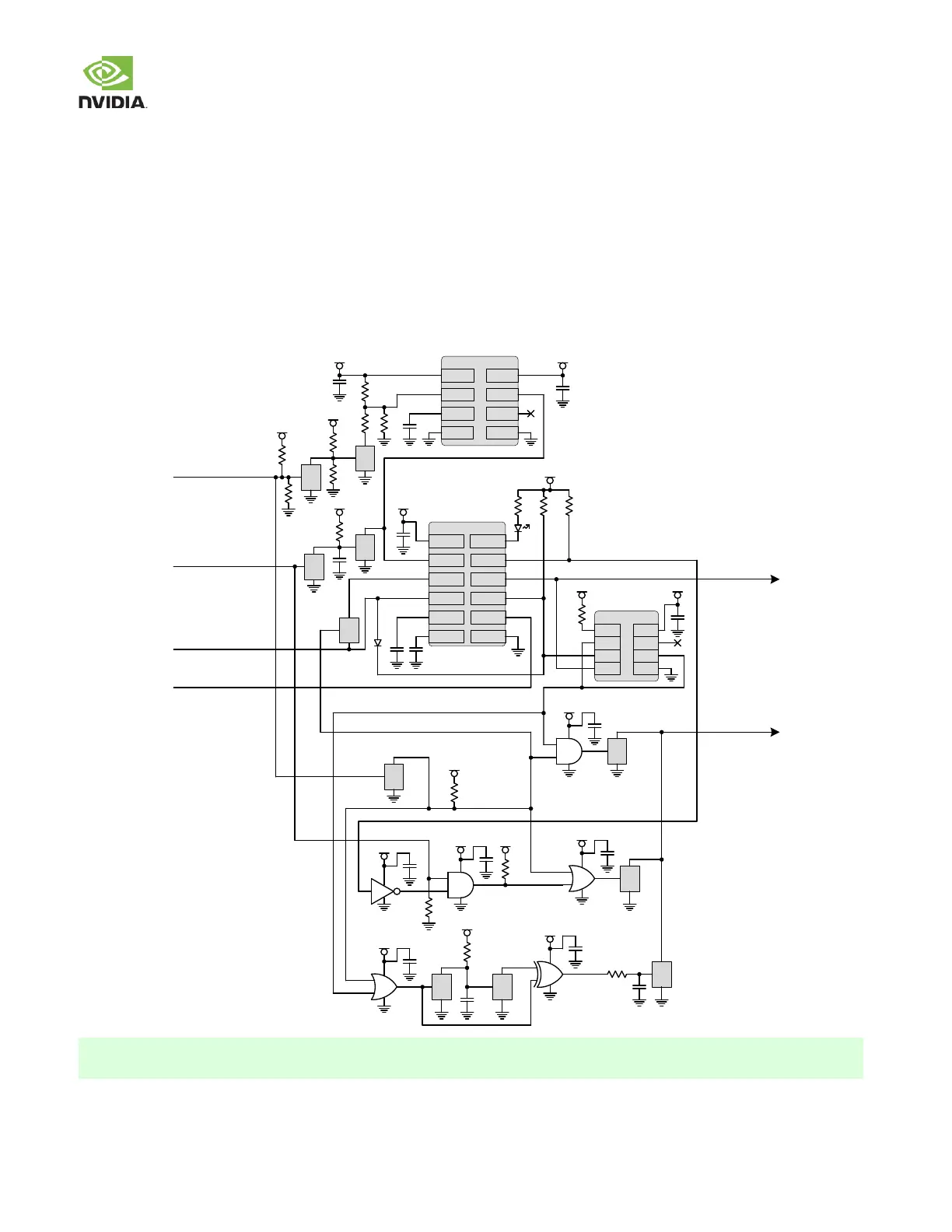
w hich is floating on Jetson TX2 w ill be grounded on the Jetson TX2i as a means to differentiate between the two module types.
The module pow er configuration identification pin (MOD_PWR_CFG_ID) resides on the Module Pin B49.
The updated carrier board, designed to support Jetson TX2i as w ell as Jetson TX2 w ill include logic that w ill use the state of the
MOD_PWR_CFG_ID pin to determine how the POWER_BTN# signal is handled. If the pin is pulled dow n due to a Jetson TX2i
module being installed, the POWER_BTN# pin w ill be driven to a steady high (ON) or low (OFF) state. If the pin is floating as
w ould be the case if a Jetson TX2 module is installed, a momentary pulse w ill be generated on the POWER_BTN# pin of the
module to initiate a pow er-on of the module. With either module type, if the system is already pow ered, a short press of the
pow er button w ill put the system in sleep mode (softw are dependent) if the system is ā€œaw ake,ā€ w ake the system if in sleep mode,
or cause a force pow er-off if the Pow er-on button is held low for approximately 8 to 10 seconds.
Figure 9. Power-on Type Detection & Control
MOD_PWR_CFG_ID
POWER_BTN
TPS7A1650
OUTIN
PGEN
DELAY FB_NC
GNDTPAD
SRC0CS25D
VCCLO*VCC
PBOUTPSHOLD
SR* EN/EN*
GND
INT*
PB*
CSRD
VREF
RST*
G
D
S
FET
G
D
S
FET
VDD_19V_IN
VDD_19V_IN
VDD_19V_IN
5V0_AO
5V0_AO
MOD_VIN_EN
WAKE_L
74LVC1G74
VCCSD
QD
CP Q*
GNDRD
5V0_AO
MOD_PWR_ON_STATE_L
5V0_AO
G
D
S
FET
CARRIER_PWR_ON
5V0_AO
5V0_AO
G
D
S
FET
G
D
S
FET
G
D
S
FET
G
D
S
FET
5V0_AO
ONOFF_CTLR_PBOUT
G
D
S
FET
G
D
S
FET
5V0_AO 5V0_AO
5V0_AO
MOD_PWR_CFG_ID_L POWER_ON
5V0_AO
5V0_AO
5V0_AO
5V0_AO
5V0_AO
From Module
Strap (Pin B49)
From Module
Pin (A48)
From Power
Button
From Module
SYS_WAKE# (Pin
B48 – TX2i only)
To main input
power FET enable
circuit (TX2i only).
To Module
POWER_BTN#
Pin (B50)
G
D
S
FET
G
D
S
FET
Note
The figure above is a high-level representation of the connections involved. Details will be provided in a future carrier
board reference design.

Other manuals for Nvidia JETSON TX2

Questions and Answers:

Question and Answer IconNeed help?

Do you have a question about the Nvidia JETSON TX2 and is the answer not in the manual?

Nvidia JETSON TX2 Specifications

General IconGeneral
BrandNvidia
ModelJETSON TX2
CategoryMicrocontrollers
LanguageEnglish

Related product manuals