EasyManuals Logo
Home>Nvidia>Microcontrollers>JETSON TX2

Nvidia JETSON TX2 User Manual

Nvidia JETSON TX2
103 pages
To Next Page IconTo Next Page
To Previous Page IconTo Previous Page
Page #17 background imageLoading...
Page #17 background image
NVIDIA Jetson TX2/TX2i OEM Product Design Guide
JETSON TX2/TX2i OEM PRODUCT | DESIGN GUIDE | 20180618 17
3.6 Power & Voltage Monitoring
3.6.1 Power Monitor
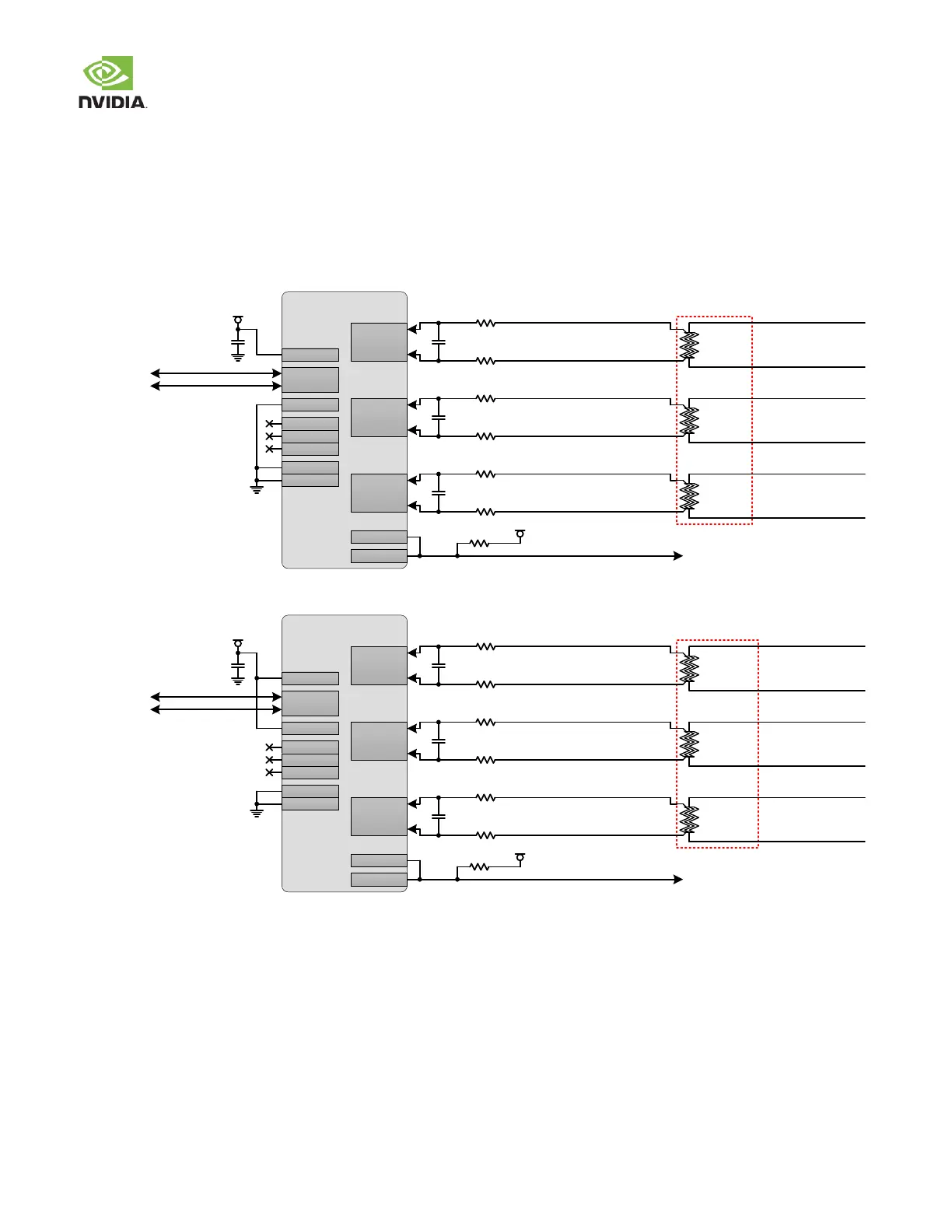
Pow er monitors are provided on the module. These monitor the main DC, CPU, GPU/SRAM, SOC (CORE) & DDR Supplies.
The monitors w ill toggle a WARN (w arning) output, or a CRIT (critical) output, depending on the pow er seen at the sense
resistors and the thresholds set for each supply.
Figure 10. Power Monitor (GPU/SRAM, SOC & WLAN)
Sense
Resistors
GEN1_I2C_SDA
GEN1_I2C_SCL
INA3221AIRGVR
Power Monitor
GPU_INA_P

0805
0.1uF
GPU_INA_M
VDD_3V3_SYS
GPU Supply Monitor
SOC Supply Monitor
Wi-Fi Supply Monitor
(Jetson TX1/TX2 Only)
GEN1_I2C
(PU to 3.3V)
SOC_INA_P

0805
SOC_INA_M
WIFI_INA_P

0603
WIFI_INA_M
10
10
10
10
10
10
VIN1P
VIN1N
WARN
CRIT
VS
AO
PV
TC
VPU
GND
SCL
SDA
PAD
VIN2P
VIN2N
VIN3P
VIN3N
Tegra GPIO_MDM6
VDD_IN
VDD_IN
VDD_SYS_SOC_IN
(SOC supply input)
VDD_SYS_GPU_IN
(GPU supply input)
VDD_3V8_WIFI_SENSE
VDD_5V0_SYS
1uF
1uF
1uF
100k
VDD_1V8
INA_WIFI_THERM_WARN_L
Figure 11. Power Monitor (VDD_IN, CPU & DDR)
Sense
Resistors
GEN1_I2C_SDA
GEN1_I2C_SCL
INA3221AIRGVR
Power Monitor
VDD_IN_SENSE

3012
0.1uF
VDD_IN_PREREG_SENSE
VDD_3V3_SYS
VDD_IN Supply Monitor
CPU Supply Monitor
DDR Supply Monitor
GEN1_I2C
(PU to 3.3V)
CPU_INA_P

0805
CPU_INA_M
SRAM_INA_P

0603
SRAM_INA_M
10
10
10
10
10
10
VIN1P
VIN1N
WARN
CRIT
VS
AO
PV
TC
VPU
GND
SCL
SDA
PAD
VIN2P
VIN2N
VIN3P
VIN3N
Tegra BATT_OC
VDD_IN_RS
VDD_IN
VDD_SYS_CPU_IN
(CPU supply input)
VDD_IN
VDD_5V0_SD0
(DDR supply input)
VDD_5V0_SYS
1uF
1uF
1uF
100k
VDD_1V8
INA_PREREG_THERM_WARN_L
3.6.2 Voltage Monitor
Jetson TX2i
A voltage monitor circuit is implemented on Jetson TX2i to indicate if the main DC input rail, VDD_IN, “droops” below an
acceptable level. The device used w ill react quickly and drive VIN_PWR_BAD# active (low ) w hich w ill force the pow er off. The
voltage monitor circuit is implemented w ith a fast voltage comparator supplied by VDD_IN w ith a 5V reference. This device has
an open drain active low output w hich is pulled low w hen the VDD_IN voltage drops below the selected threshold (8.04V).

Other manuals for Nvidia JETSON TX2

Questions and Answers:

Question and Answer IconNeed help?

Do you have a question about the Nvidia JETSON TX2 and is the answer not in the manual?

Nvidia JETSON TX2 Specifications

General IconGeneral
BrandNvidia
ModelJETSON TX2
CategoryMicrocontrollers
LanguageEnglish

Related product manuals