NVIDIA Jetson TX2/TX2i OEM Product Design Guide
JETSON TX2/TX2i OEM PRODUCT | DESIGN GUIDE | 20180618 90
18.0 APPENDIX C: TRANSMISSION LINE PRIMER
18.1 Background
NVIDIA maintains strict guidelines for high-frequency PCB transmission lines to ensure optimal signal integrity for data
transmission. This section provides a brief primer into basic board-level transmission line theory.
Characteristics
The most important PCB transmission line characteristics are listed in the follow ing bullets:
▪ Trace w idth/height, PCB height and dielectric constant, and layer stack-up affect the characteristic trace
impedance of a transmission line.
▪ Signal rise time is proportional to the transmission line impedance and load capacitance.
* C
Load
RiseTime =
Z
0
* R
Term
Z
0
+ R
Term
˜
▪ Real transmission lines (Figure 50) have non-zero resistances that lead to attenuation and distortion, creating
signal integrity issues.
Figure 50. Typical Transmission Line Circuit
Transmission Line
Z
S
Z
0
Z
L
LoadSource
Transmission lines are used to “transmit” the source signal to the load or destination w ith as little signal degradation or reflection
as possible. For this reason it is important to design the high-speed signal transmission line to fall w ithin characteristic guidelines
based on the signal speed and type.
18.2 Physical Transmission Line Types
The tw o primary transmission line types often used for module board designs are:
▪ Microstrip transmission line (Figure 51)
▪ Stripline transmission line (Figure 52)
The follow ing sections describe each type of transmission.
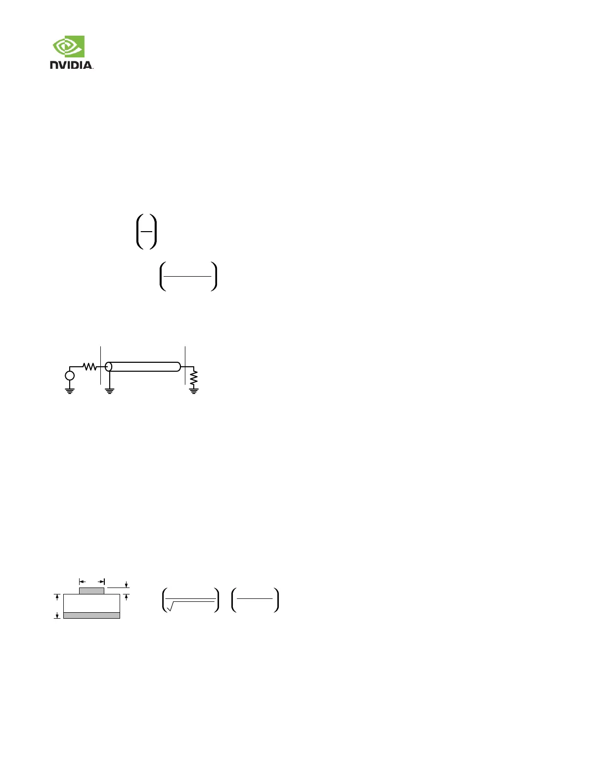
Microstrip Transmission Line
Figure 51. Microstrip Transmission Line
Dielectric
W
TH
Z
0
=
ln
87
Er + 1.414
5.98H
0.8W + T
▪ Z
0
: Impedance
▪ W: Trace w idth (inches)
▪ T: Trace thickness (inches)
▪ Er: Dielectric constant of substrate
▪ H: Distance betw een signal and reference plane
Stripline Transmission Line
 Loading...