NVIDIA Jetson TX2/TX2i OEM Product Design Guide
JETSON TX2/TX2i OEM PRODUCT | DESIGN GUIDE | 20180618 72
GND &
0.1uF to GND (on the module)
JTAG General Purpose Pin #0: Connect to TRST pin of connector
GND (on the module)
JTAG General Purpose Pin #1: Used as select
- Normal operation: Leave series resistor from NVJTAG_SEL not stuffed.
- Scan test mode: Connect NVJTAG_SEL to VDD_1V8 (install 0Ω resistor as
shown).
12.6.2 Debug UART
Jetson TX2/TX2i provides UART0 for debug purposes. The connections are show n in Figure 44 and described in the table
below .
Table 85. Debug UART Connections
UART #0 Transmit: Connect to RX pin of serial device
on the non-the module side of the device.
UART #0 Receive: Connect to TX pin of serial device
GND or VDD_1V8 on the module for
RAM Code strapping
UART #0 Request to Send: Connect to CTS pin of serial device
If level sh
on the non-the module side of the device.
UART #0 Clear to Send: Connect to RTS pin of serial device
12.6.3 Boundary Scan Test Mode
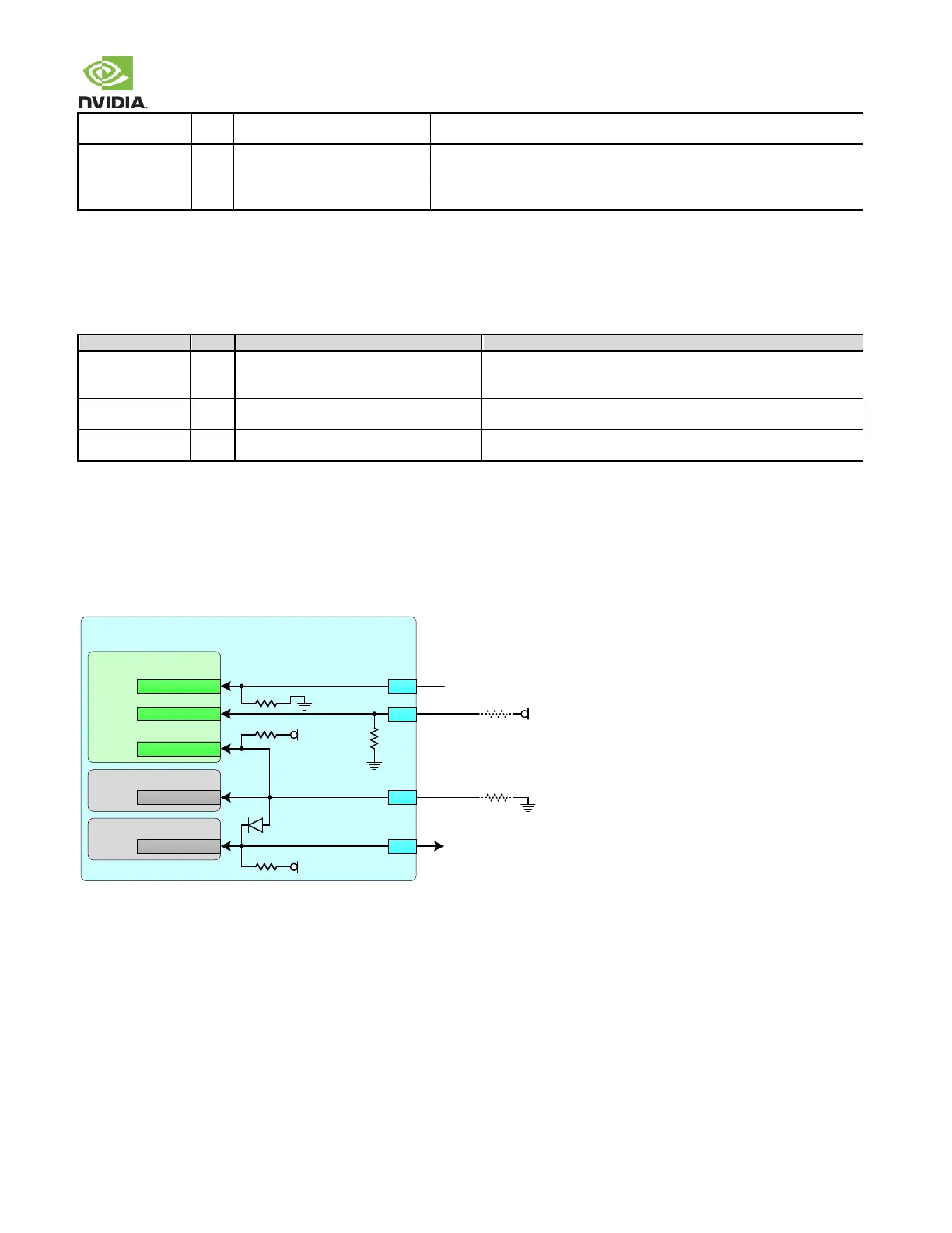
To support Boundary Scan Test mode, the Tegra NVJTAG_SEL pin must be pulled high and Tegra must be held in reset
w ithout resetting the PMIC. The figure below illustrates this. Other requirements related to supporting Boundary Scan Test
mode are described in the “Tegra X2 Boundary Scan Requirements & Usage” document.
Figure 45. Boundary Scan Connections
Jetson TX2/TX2i
PMIC
Tegra
Devices requiring system reset
& System Reset Sources
VDD_1V8
R1 - 0Ω
Leave Resistors R1 & R2 uninstalled
for normal operation. Install both
for boundary scan test mode.
100kΩ
100kΩ
VDD_1V8
eMMC
R2 - 0Ω
JTAG_TRST_N
SYS_RESET_N
RESET*
RST I/O
JTAG_GP0
A46
RESET_OUT#
A47
RESET_IN#
10kΩ
1.8V
NVJTAG_SEL
A11
JTAG_GP1
TRST on JTAG ConnectorB1 3
100kΩ
12.7 Strapping Pins
Jetson TX2/TX2i has one strap (FORCE_RECOV#) that is intended to be used on the carrier board. That strap is used to enter
Force Recovery mode. The other straps mentioned in this section are for use on the module by Nvidia only. They are included
here as their state at power-on must be kept at the level selected on the module.
 Loading...