NVIDIA Jetson TX2/TX2i OEM Product Design Guide
JETSON TX2/TX2i OEM PRODUCT | DESIGN GUIDE | 20180618 18
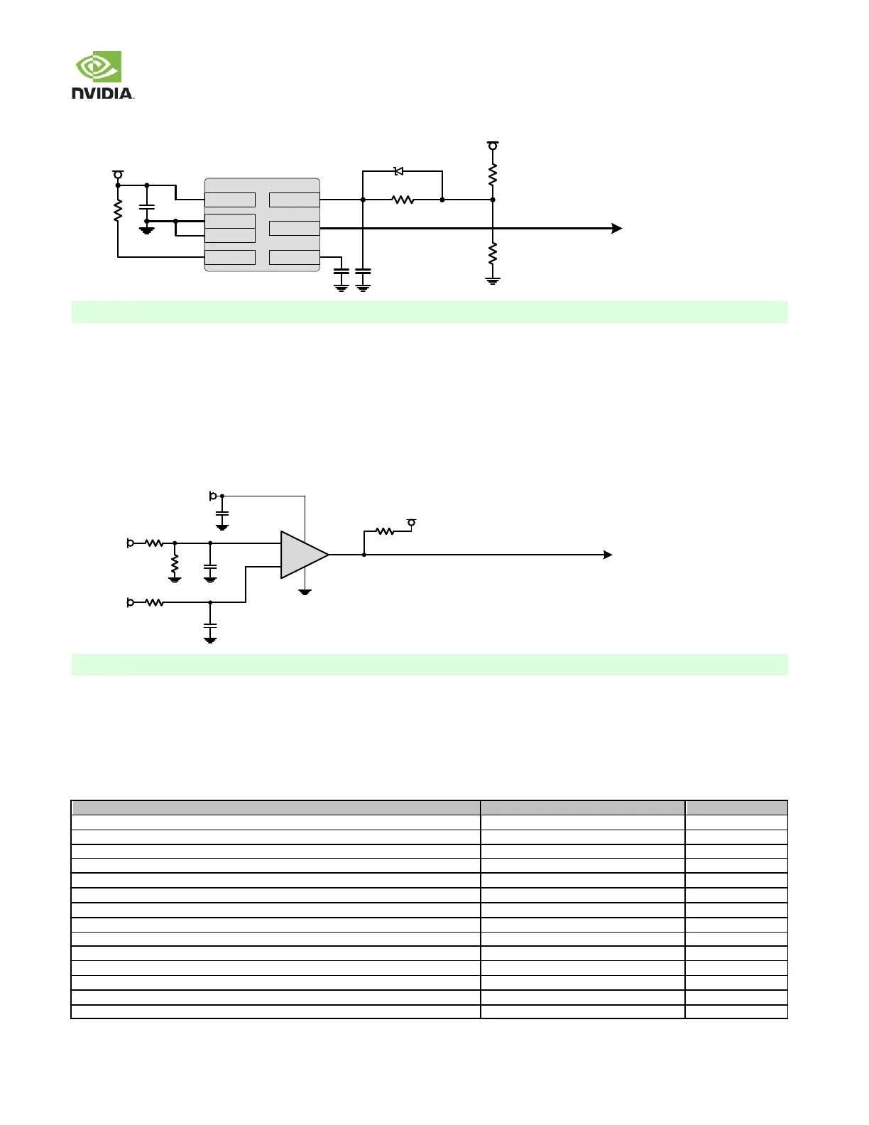
Figure 12. Voltage Monitor Connections
VDD_IN
47.5k
1%
47.4k,1%
VIN_PWR_BAD#
TPS3808G01
TP
SENSE
CT
VCC
MR*
GND
RST*
2.49k
1%
100k
1%
RB521CS30L
The threshold for VDD_IN, determined by the voltage divider components used in the circuit above is 8.04V.
Jetson TX2
A voltage monitor circuit is implemented on Jetson TX2 to indicate if the main DC input rail, VDD_IN, “droops” below an
acceptable level. The device used w ill react quickly and generate an alert to one of the Tegra SOC_THERM capable pins
(VCOMP_ALERT). The voltage monitor circuit is implemented w ith a fast voltage comparator supplied by VDD_IN w ith a 1.8V
(VDD_1V8) reference common w ith the Tegra IO domain that receives the output signal. This device has an open drain active
low output w hich is pulled low w hen the VDD_IN voltage drops below the selected threshold.
Figure 13. Voltage Monitor Connections
VDD_IN
VDD_1V8
VDD_5V0_SYS
34k,1%34k,1%
49.9k
1%
49.9k
1%
110k,1%110k,1%
COMP_SOC_THERM* (Tegra VCOMP_ALERT)VOUT
IN_POS
IN_NEG
VCC
VEE
+
VOUT
IN_POS
IN_NEG
VCC
VEE
+
100k100k
1.8V
The threshold for VDD_IN, determined by the voltage divider components used in the cir cuit above is 5.75V.
3.7 Deep Sleep (SC7)
Jetson TX2/TX2i supports a low pow er state called Deep Sleep or SC7. This can be entered under softw are control, and exited
using various mechanisms, including wake capable pins that are listed in the table below .
Table 11. Signal Wake Events
Potential Wake Event (Reference Design Signal)
PCIe Wake Request (PEX_WAKE#)
Bluetooth Wake AP (BT2_WAKE_AP Secondary)
WLAN Wake AP (WIFI_WAKE_AP - Secondary)
Thermal/Over-current Warning
Audio Codec Interrupt (AUD_INT_L)
DP 0 Hot Plug Detect (DP_AUX_CH0_HPD)
HDMI Consumer Electronic Control (HDMI_CEC)
DP 1 Hot Plug Detect (DP_AUX_CH1_HPD)
Camera Vertical Sync (CAM_VSYNC)
Motion Interrupt (MOTION_INT)