NVIDIA Jetson TX2/TX2i OEM Product Design Guide
JETSON TX2/TX2i OEM PRODUCT | DESIGN GUIDE | 20180618 71
12.6 Debug
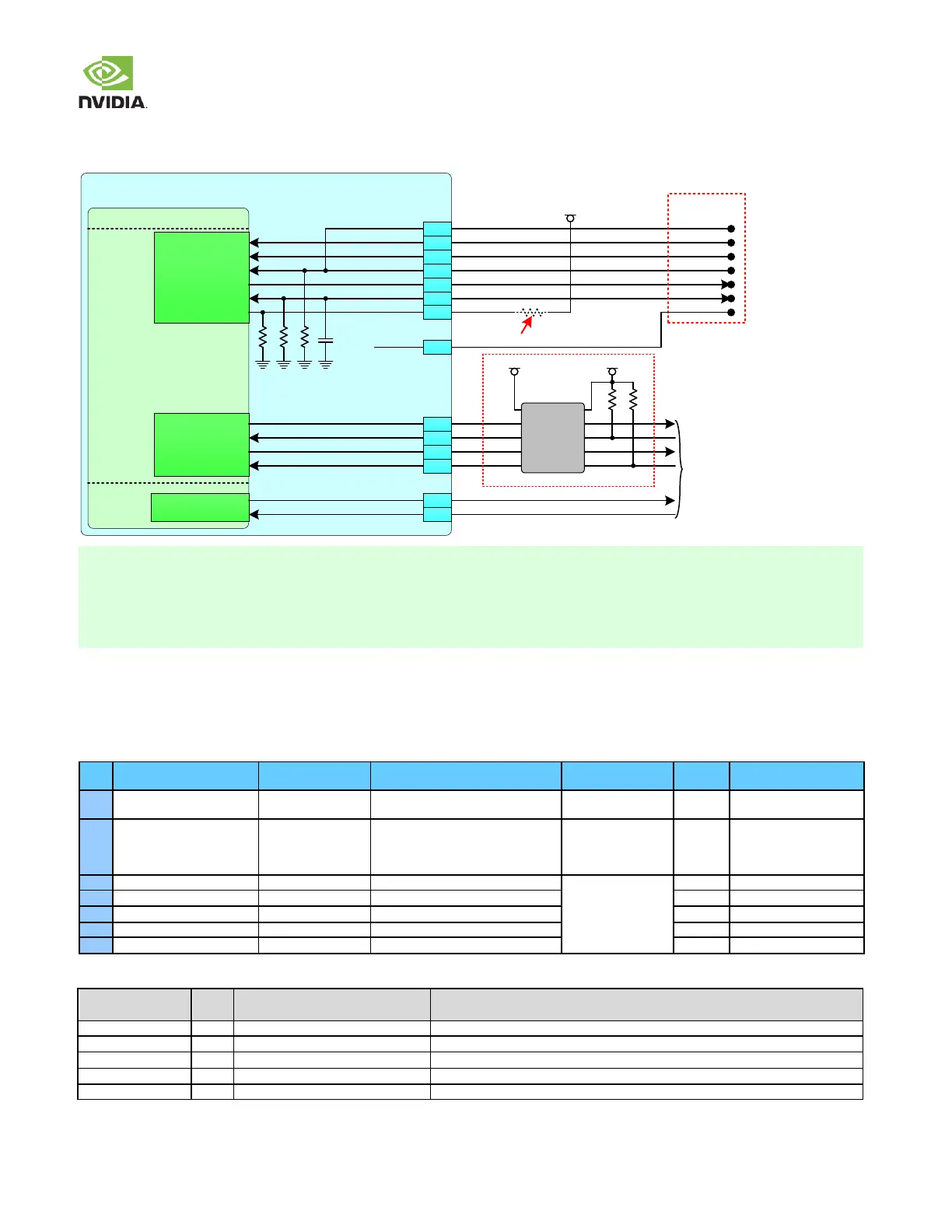
Figure 44. Debug Connections
Jetson TX2/TX2i
Tegra
JTAG_TMS
JTAG_TDI
JTAG_TCK
JTAG_TDO
JTAG_TRST_N
NVJTAG_SEL
100kΩ
UART1_TXD
UART1_RXD
UART1_RTS_N
UART1_CTS_N
For Debug Use
DEBUG
0.1uF
A12
A14
B1 2
B1 1
A13
G12
H12
B1 3
JTAG_RTCK
JTAG_TMS
JTAG_TDI
JTAG_TCK
JTAG_TDO
JTAG_GP0
JTAG_GP1
RESET_IN
UART0_TX
UART0_RX
UART0_RTS#
UART0_CTS#
RSVD
RSVD
100kΩ
See Note 1
Optional JTAG
connections
0
A47
To PMIC
RTCK
TMS
TDI
TCLK
TDO
TRST_N
RST
A11
H11
G11
VDD_1V8
100kΩ
UART7_TX
UART7_RX
DP
D5
D8
See Note 2
Level
Shifter
100k
VDD_3V3_SYSVDD_1V8
100k
1. JTAG_GP1 (Tegra NVJTAG_SEL) is left unconnected (pulled down on module) for normal operation and pulled to 1.8V for
Boundary Scan Mode.
2. If level shifter is implemented, pull-ups are required the RX & CTS lines on the non-Tegra side of the level shifter. This is
required to keep the inputs from floating and toggling when no device is connected to the debug UART.
3. Check preferred JTAG debugger documentation for JTAG PU/PD recommendations.
12.6.1 JTAG
JTAG is not required, but may be useful for new design bring-up or for Boundary Scan.
Table 83. JTAG Pin Descriptions
Usage on the Carrier
Board
JTAG Header & Debug
Connector
JTAG General Purpose 1. Pulled low on
module for normal operation & pulled
high by test device for Boundary Scan
test mode.
JTAG Header & Debug
Connector
Table 84. JTAG Signal Connections
Module Pin
(function) Name
JTAG Mode Select: Connect to TMS pin of connector
100GND (on the module)
JTAG Clock: Connect to TCK pin of connector
JTAG Data Out: Connect to TDO pin of connector
JTAG Data In: Connect to TDI pin of connector
JTAG Return Clock: Connect to RTCK pin of connector
 Loading...