EasyManuals Logo
Home>Nvidia>Microcontrollers>JETSON TX2

Nvidia JETSON TX2 User Manual

Nvidia JETSON TX2
103 pages
To Next Page IconTo Next Page
To Previous Page IconTo Previous Page
Page #38 background imageLoading...
Page #38 background image
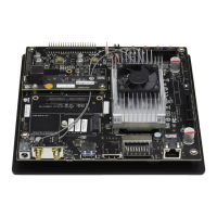
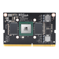
NVIDIA Jetson TX2/TX2i OEM Product Design Guide
JETSON TX2/TX2i OEM PRODUCT | DESIGN GUIDE | 20180618 38
7.0 DISPLAY
Jetson TX2/TX2i designs can select from several display options including MIPI DSI & eDP for embedded displays, and HDMI
or DP for external displays. Three display controllers are available, so the possible display combinations are:
DP/HDMI + eDP + single/dual-link-DSI
DP/HDMI + single-link-DSI + single-link-DSI
DP/HDMI + DP/HDMI + single/dual-link-DSI
Table 33. Display General Pin Descriptions
Pin #
Module Pin Name
Tegra Signal
Usage/Description
Usage on Carrier Board
Direction
Pin Type
A26
GSYNC_HSYNC
GPIO_DIS4
GSYNC Horizontal Sync
Display Connector
Output
CMOS 1.8V
A27
GSYNC_VSYNC
GPIO_DIS2
GSYNC Vertical Sync
Output
CMOS 1.8V
A25
LCD_TE
GPIO_DIS1
Display Tearing Effect
Input
CMOS 1.8V
B26
LCD_VDD_EN
GPIO_EDP0
Display VDD Enable
Output
CMOS 1.8V
B28
LCD_BKLT_EN
GPIO_DIS3
Display Backlight Enable
Output
CMOS 1.8V
B27
LCD0_BKLT_PWM
GPIO_DIS0
Display Backlight PWM 0
Output
CMOS 1.8V
A24
LCD1_BKLT_PWM
GPIO_DIS5
Display Backlight PWM 1
Output
CMOS 1.8V
7.1 MIPI DSI
Jetson TX2/TX2i supports eight total MIPI DSI data lanes. Each data lane has a peak bandw idth up to 1.5Gbps. The lanes can
be configured in Dual Link & Split Link modes. The follow ing configurations are possible:
Dual Link Mode (Up to 8 PHY lanes):
DSI-A (1x4) + DSI-C (1x4) to single display
DSI-A (1x4) to one display, DSI-C (1x4) to a second display
Split Link Mode (Up to 8 PHY lanes):
Two Links with 1-lane each: DSI-A(1x1) + DSI-B (1x1) or DSI-C (1x1) + DSI-D (1x1)
Two Links with 2-lane each: DSI-A(1x2) + DSI-B (1x2) or DSI-C (1x2) + DSI-D (1x2)
Four Links with 1-lane each: DSI-A(1x1) + DSI-B (1x1) + DSI-C (1x1) + DSI-D (1x1)
Four Links with 2-lane each: DSI-A(1x2) + DSI-B (1x2) + DSI-C (1x2) + DSI-D (1x2)
Table 34. DSI Pin Descriptions
Pin #
Module Pin Name
Tegra Signal
Usage/Description
Usage on Carrier Board
Direction
Pin Type
G34
DSI0_CLK
DSI_A_CLK_N
Display, DSI 0 Clock
Display Connector
Output
MIPI D-PHY
G33
DSI0_CLK+
DSI_A_CLK_P
Display, DSI 0 Clock+
Output
F35
DSI0_D0
DSI_A_D0_N
Display, DSI 0 Data 0
Output
F34
DSI0_D0+
DSI_A_D0_P
Display, DSI 0 Data 0+
Output
H33
DSI0_D1
DSI_A_D1_N
Display, DSI 0 Data 1
Output
H32
DSI0_D1+
DSI_A_D1_P
Display, DSI 0 Data 1+
Output
D34
DSI1_CLK
DSI_B_CLK_N
Display DSI 1 Clock
Output
D33
DSI1_CLK+
DSI_B_CLK_P
Display DSI 1 Clock+
Output
C35
DSI1_D0
DSI_B_D0_N
Display, DSI 1 Data 0
Output
C34
DSI1_D0+
DSI_B_D0_P
Display, DSI 1 Data 0+
Output
E33
DSI1_D1
DSI_B_D1_N
Display, DSI 1 Data 1
Output
E32
DSI1_D1+
DSI_B_D1_P
Display, DSI 1 Data 1+
Output
G31
DSI2_CLK
DSI_C_CLK_N
Display DSI 2 Clock
Output
G30
DSI2_CLK+
DSI_C_CLK_P
Display DSI 2 Clock+
Output
F32
DSI2_D0
DSI_C_D0_N
Display, DSI 2 Data 0
Output
F31
DSI2_D0+
DSI_C_D0_P
Display, DSI 2 Data 0+
Output
H30
DSI2_D1
DSI_C_D1_N
Display, DSI 2 Data 1
Output
H29
DSI2_D1+
DSI_C_D1_P
Display, DSI 2 Data 1+
Output
D31
DSI3_CLK
DSI_D_CLK_N
Display DSI 3 Clock
Output
D30
DSI3_CLK+
DSI_D_CLK_P
Display DSI 3 Clock+
Output
C32
DSI3_D0
DSI_D_D0_N
Display, DSI 3 Data 0
Output
C31
DSI3_D0+
DSI_D_D0_P
Display, DSI 3 Data 0+
Output
E30
DSI3_D1
DSI_D_D1_N
Display, DSI 3 Data 1
Output
E29
DSI3_D1+
DSI_D_D1_P
Display, DSI 3 Data 1+
Output

Other manuals for Nvidia JETSON TX2

Questions and Answers:

Question and Answer IconNeed help?

Do you have a question about the Nvidia JETSON TX2 and is the answer not in the manual?

Nvidia JETSON TX2 Specifications

General IconGeneral
BrandNvidia
ModelJETSON TX2
CategoryMicrocontrollers
LanguageEnglish

Related product manuals