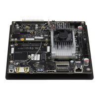
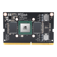
NVIDIA Jetson TX2/TX2i OEM Product Design Guide
JETSON TX2/TX2i OEM PRODUCT | DESIGN GUIDE | 20180618 57
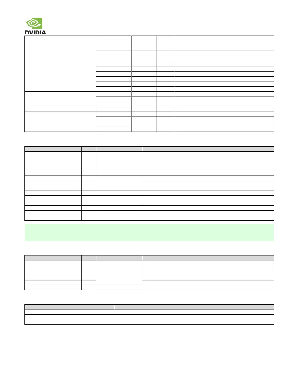
UHS50 Card = optional, UHS104 Card = mandatory
UHS50 Card = mandatory, UHS104 Card = mandatory
UHS50 Card = optional, UHS104 Card = mandatory
UHS50 Card = optional, UHS104 Card = mandatory
F
MAX
(CLK base frequency)
Single data rate up to 104MB/sec
Double data rate up to 50MB/sec
Single data rate up to 50MB/sec
Single data rate up to 25MB/sec
Single data rate up to 12.5MB/sec
Single data rate up to 25MB/sec
Single data rate up to 12.5MB/sec
C
LOAD
(C
CARD
+C
EQ
)
(CLK freq = 208MHz)
Total load capacitance supported
Total load capacitance supported
Total load capacitance supported
Possibly 22pF+ depending on host system
C
LOAD
(C
CARD
+C
EQ
)
(CLK freq = 100/50/25MHz)
Total load capacitance supported
Total load capacitance supported
Total load capacitance supported
Possibly 22pF+ depending on host system
Table 56. SDCARD Signal Connections
120 bead on module
for SDCARD_CLK. 0
series resistor on carrier
board as placeholder.
See note for EMI/ESD
SDIO/SD Card Clock: Connect to CLK pin of device or socket
10 series resistors for
SDCARD CMD/D[3:0].
See note for EMI/ESD
SDIO/SD Card Command: Connect to CMD pin of device/socket
SDIO/SD Card Data: Connect to Data pins of device or socket
SD Card Card Detect: Connect to CD/C_DETECT pin on socket if required.
SD Card Write Protect: Connect to WP/WR_PROTECT pin on socket if
required.
SDIO Reset: Connect to reset line on SDIO peripheral/connector.
SD Card Supply/Load Switch Enable: Connect to enable of supply/load switch
supplying VDD on SD Card socket.
EMI/ESD may be required for SDIO when used as the SD Card socket interface. Any EMI/ESD device used must be able to meet signal
timing/quality requirements. The Carrier Board implements 10 series resistors on the SDCARD data lines and a 0 series resistor on the
clock line (for possible tuning if required).
Table 57. SDIO Signal Connections (Jetson TX2i only)
120 bead on module
for SDCARD_CLK. See
note for EMI/ESD
SDIO/SD Card Clock: Connect to CLK pin of device or socket
SDIO/SDMMC Command: Connect to CMD pin of device/socket
SDIO/SDMMC Data: Connect to Data pins of device or socket
SDIO Reset: Connect to reset line on SDIO peripheral/connector.
Table 58. Recommended SDCARD/SDIO observation (test) points for initial boards
One for SDCARD/SDIO_CLK line.
Near Device/Connector pin. SD connector pin can be used for device end if accessible.
One SDCARD/SDIO_DATx line & one for
SDCARD/SDIO_CMD.
Near the module & Device pins. SD connector pin can be used for device end if accessible.
 Loading...