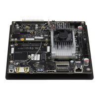
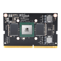
NVIDIA Jetson TX2/TX2i OEM Product Design Guide
JETSON TX2/TX2i OEM PRODUCT | DESIGN GUIDE | 20180618 59
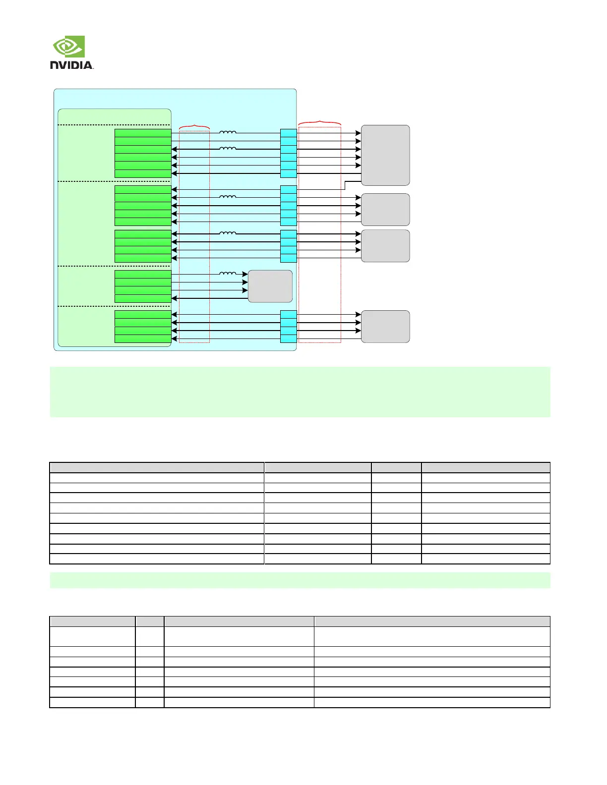
Figure 32. I2S & Codec Clock/Control Connections
Jetson TX2/TX2i
Audio
Codec
Tegra
DAP2_SCLK
DAP1_SCLK
GPIO_PQ0
AUDIO
DMIC_HV
2
nd
WiFi/BT,
Modem
Misc
DMIC2_DAT
DAP1_FS
DAP1_DOUT
DAP1_DIN
GPIO_PQ3
GPIO_PQ1
GPIO_PQ2
DMIC1_CLK
DMIC2_CLK
DMIC1_DAT
DAP2_FS
DAP2_DOUT
DAP2_DIN
AUDIO_MCLK
GPIO19_AUD_RST
I2S0_CLK
I2S0_LRCK
I2S0_SDOUT
I2S0_SDIN
GPIO20_AUD_INT
I2S2_CLK
I2S2_LRCK
I2S2_SDOUT
I2S2_SDIN
I2S3_CLK
I2S3_LRCK
I2S3_SDOUT
I2S3_SDIN
I2S1_CLK
I2S1_LRCK
I2S1_SDOUT
I2S1_SDIN
Primary
WiFi/BT
(TX2 only)
AUDIO_I2S_MCLK
GPIO_X1_AUD
DAP1_SCLK_AP
DAP1_FS_AP
DAP1_DOUT_AP
DAP1_DIN_AP
AUD_INT
DAP3_SCLK_AP
DAP3_FS_AP
DAP3_DOUT_AP
DAP3_DIN_AP
DAP4_SCLK_AP
DAP4_FS_AP
DAP4_DOUT_AP
DAP4_DIN_AP
DAP2_SCLK_AP
DAP2_FS_AP
DAP2_DOUT_AP
DAP2_DIN_AP
CONN
AUD_MCLK
GPIO_AUD0
GPIO_AUD1
F2
F1
D14
D13
C14
G2
H1
H2
G1
G5
H3
H5
H6
G6
C15
AUDIO_HV
I2S1_CLK
I2S1_LRCK
I2S1_SDOUT
I2S1_SDIN
I2S3_CLK
I2S3_LRCK
I2S3_SDOUT
I2S3_SDIN
I2S4_CLK
I2S4_LRCK
I2S4_SDOUT
I2S4_SDIN
I2S6_CLK
I2S6_LRCK
I2S6_SDOUT
I2S6_SDIN
I2S2_CLK
I2S2_LRCK
I2S2_SDOUT
I2S2_SDIN
Tegra
Function
DAP4_SCLK
DAP4_FS
DAP4_DOUT
DAP4_DIN
E6
F5
F6
E5
Misc
Nvidia
Carrier Board
Net Name
- The I2S interfaces can be used in either Master or Slave mode.
- A capacitor from DAPn_FS to GND is recommended if Tegra an I2S slave & the edge_cntrl configuration = 1 (SDATA
driven on positive edge of SCLK). The value of the capacitor should be chosen to provide a minimum of 2ns hold time for
the DAPn_FS edge after the rising edge of DAPn_SCLK.
I2S Design Guidelines
Table 61. I2S Interface Signal Routing Requirements
Configuration / Device Organization
Breakout Region Impedance
Via proximity (Signal to reference)
Trace spacing Microstrip or Stripline
Max Trace Delay Skew between SCLK & SDATA_OUT/IN
Up to 4 signal Vias can share a single GND return Via
Table 62. I2S & Codec Clock/Control Signal Connections
I2S[2,0]_CLK have 75 beads & I2S3_CLK
has a 120on the module).
I2S Serial Clock: Connect to I2S/PCM CLK pin of audio device.
I2S Left/Right Clock: Connect to Left/Right Clock pin of audio device.
I2S Data Output: Connect to Data Input pin of audio device.
I2S Data Input: Connect to Data Output pin of audio device.
75the module).
Audio Codec Master Clock: Connect to clock pin of Audio Codec.
Audio Reset: Connect to reset pin of Audio Codec.
Audio Interrupt: Connect to interrupt pin of Audio Codec.
 Loading...