3939
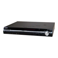
HCD-DX375
HCD-DX375
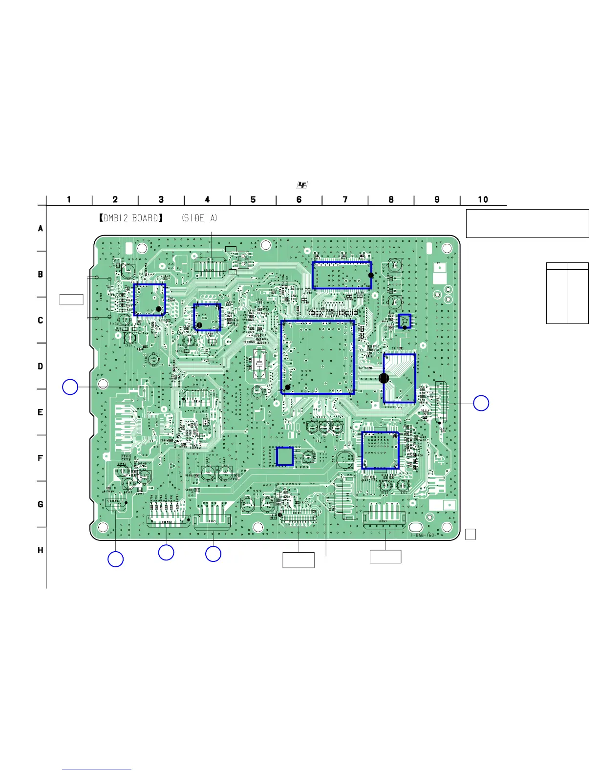
6-6. PRINTED WIRING BOARD – DMB12 BOARD (SIDE A) –
• See page 33 for Circuit Boards Location.
:Uses unleaded solder.
• Semiconductor
Location
Ref. No.
Location
IC101 D-6
IC102 D-8
IC103 C-8
IC104 B-7
IC110 F-6
IC201 F-8
IC701 C-3
IC708 C-4
Q101 G-6
Q103 G-6
✩ New part of EEP ROM (IC103, IC706) on the DMB12 board
cannot be used.
Therefore, if the mounted MAIN board (A-1148-813-A) is
replaced, exchange new EEP ROM (IC103, IC706) with that used
before the replacement.
MAIN BOARD
CN701
(Page 49)
O
I/O BOARD
CN202
(Page 56)
C
I/O BOARD
CN201
(Page 56)
B
MAIN BOARD
CN505
(Page 49)
N
MAIN BOARD
CN504
(Page 48)
P
SPINDLE MOTOR
SLED MOTOR
for DIAG JIG
OPTICAL PICK-UP
BLOCK
(KHM-310CAB)
IC701
IC708
IC101
IC110
IC201
IC104
IC102
IC103
HDMI OUT
(DVD ONLY)
for CHECK
NOM
DL
16
S1
D2
S2
D1
E
1
3
8
2
9
12
 Loading...