10 www.xilinx.com AC701 Evaluation Board
UG952 (v1.3) April 7, 2015
Chapter 1: AC701 Evaluation Board Features
Feature Descriptions
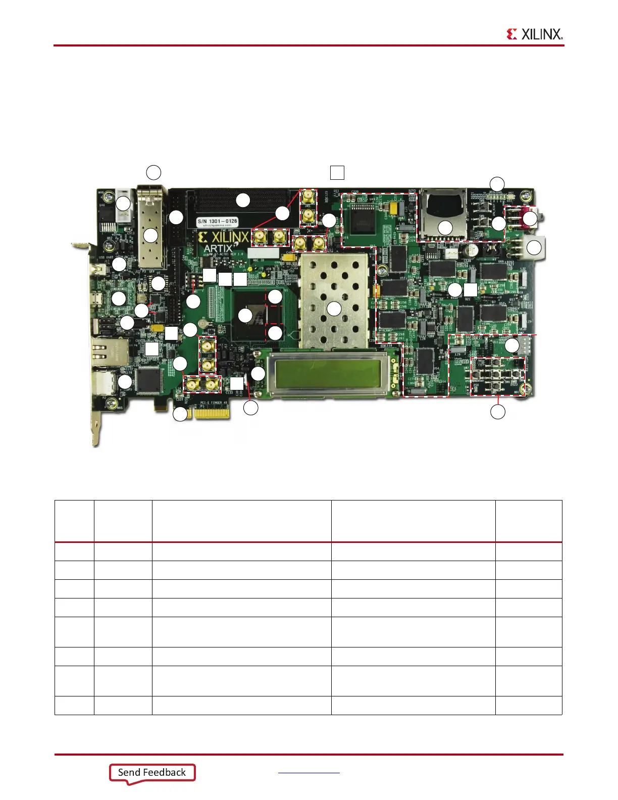
Figure 1-2 shows the AC701 board. Each numbered feature that is referenced in Figure 1-2
is described in the sections that follow.
Note: The image in Figure 1-2 is for reference only and might not reflect the current revision of the
board.
X-Ref Target - Figure 1-2
Figure 1-2: AC701 Board Components (Rev. 2.0)
UG952_c1_02_022715
18
29
30
31
13
5
14
1
6
7
30
11
11
8
9
32
10
3
16
17
12
15
2
25
00
Square callout references a component
on the back side of the board
Round callout references a component
on the front side of the board
00
4
26
23
21
28
22
24
19
27
33
34
35
20
Table 1-1: AC701 Board Component Descriptions
Callout
Reference
Designator
Component Description Notes
Schematic
0381502
Page Number
1 U1 Artix-7 FPGA Xilinx XC7A200T-2FBG676C
2 J1 DDR3 SODIMM socket with memory Micron MT8JT12864HZ-1G6G1 10
3 U7 Quad SPI flash memory Micron N25Q256A13ESF40G 4
4 U29 SD card interface connector Molex 67840-8001 14
5 U26 USB-JTAG module
Digilent USB JTAG module (with
micro-B receptacle)
4
6 U51 System clock source (back side of board) SiTime SIT9102AI-243N25E200.0000 3
7 U34
Programmable user clock source
10 MHz-810 MHz (back side of board)
Silicon Labs SI570BAB000544DG
(default 156.250 MHz)
3
8 J31, J32 SMA user clock input Rosenberger 32K10K-400L5 3

 Loading...


